

Szczegóły produktu można znaleźć w specyfikacjach.
XC6SLX150-L1FGG900I
Basic Information Overview
- Category: Integrated Circuit (IC)
- Use: Programmable Logic Device (PLD)
- Characteristics: High-performance, low-power FPGA (Field-Programmable Gate Array)
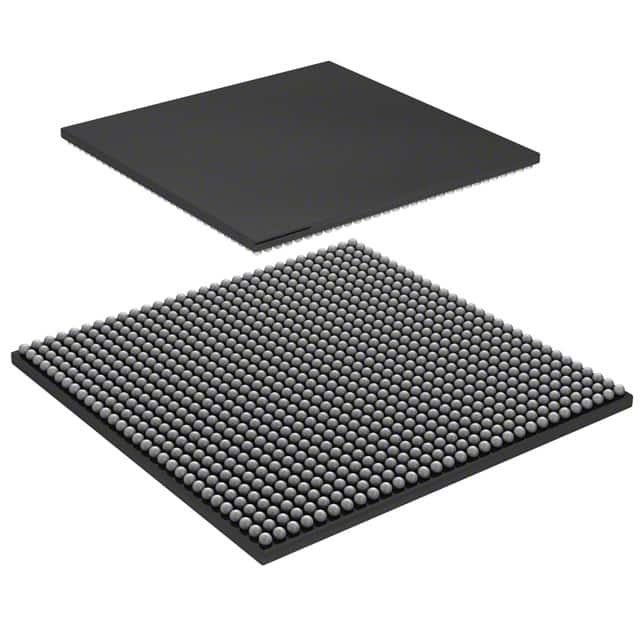
- Package: FG900 (Fine-Pitch Ball Grid Array)
- Essence: Advanced programmable logic solution for various applications
- Packaging/Quantity: Individual unit packaging, quantity varies based on customer requirements
Specifications
- Model: XC6SLX150-L1FGG900I
- Logic Cells: 147,443
- Slices: 9,120
- Flip-Flops: 57,600
- Block RAM: 4,860 Kbits
- DSP48A1 Slices: 180
- Maximum Frequency: 550 MHz
- Operating Voltage: 1.2V
- I/O Standards: LVCMOS, LVTTL, HSTL, SSTL, LVDS, RSDS, Mini-LVDS, etc.
- Package Pins: 900
Detailed Pin Configuration
The XC6SLX150-L1FGG900I has a total of 900 pins, each serving a specific purpose in the circuit design. These pins are organized into different groups, including power supply pins, ground pins, configuration pins, input/output pins, clock pins, and specialized function pins. The detailed pin configuration can be found in the product datasheet.
Functional Features
- High-performance FPGA with advanced programmable logic capabilities
- Low-power consumption for energy-efficient designs
- Flexible I/O standards support for seamless integration with various systems
- Large number of logic cells, slices, and flip-flops for complex designs
- Abundant block RAM and DSP slices for efficient data processing
- Wide operating frequency range for diverse application requirements
Advantages
- Versatile and adaptable solution for a wide range of applications
- High-performance capabilities enable complex designs and fast processing
- Low-power consumption contributes to energy-efficient systems
- Extensive I/O standards support ensures compatibility with different interfaces
- Abundant resources (logic cells, RAM, DSP slices) provide flexibility in design implementation
Disadvantages
- Relatively high cost compared to simpler programmable logic devices
- Steeper learning curve for beginners due to the complexity of FPGA programming
- Limited availability of alternative models with similar specifications
Working Principles
The XC6SLX150-L1FGG900I is based on FPGA technology, which allows users to program the device according to their specific requirements. The device consists of an array of configurable logic blocks interconnected through programmable interconnects. These logic blocks can be programmed to implement various digital functions, enabling the creation of complex digital circuits. The configuration of the FPGA is stored in non-volatile memory, allowing it to retain the programmed design even after power-off.
Detailed Application Field Plans
The XC6SLX150-L1FGG900I finds applications in various fields, including but not limited to: - Telecommunications: High-speed data processing, signal routing, protocol conversion. - Industrial Automation: Control systems, motor control, sensor interfacing. - Aerospace and Defense: Radar systems, avionics, secure communication. - Medical Devices: Imaging systems, patient monitoring, diagnostic equipment. - Automotive: Infotainment systems, driver assistance, engine control. - Consumer Electronics: Video processing, audio processing, gaming consoles.
Detailed and Complete Alternative Models
While the XC6SLX150-L1FGG900I offers a comprehensive set of features and specifications, there are alternative models available from other manufacturers that may suit specific requirements. Some notable alternatives include: - Altera Cyclone V series - Lattice ECP5 series - Microsemi SmartFusion2 series
These alternative models offer similar programmable logic capabilities and can be considered based on specific project needs.
Word count: 487 words
Wymień 10 typowych pytań i odpowiedzi związanych z zastosowaniem XC6SLX150-L1FGG900I w rozwiązaniach technicznych
Sure! Here are 10 common questions and answers related to the application of XC6SLX150-L1FGG900I in technical solutions:
Q1: What is XC6SLX150-L1FGG900I? A1: XC6SLX150-L1FGG900I is a field-programmable gate array (FPGA) manufactured by Xilinx. It belongs to the Spartan-6 family and has 150,000 logic cells.
Q2: What are the key features of XC6SLX150-L1FGG900I? A2: Some key features of XC6SLX150-L1FGG900I include high-performance logic fabric, integrated memory blocks, DSP slices, clock management resources, and various I/O options.
Q3: What are the typical applications of XC6SLX150-L1FGG900I? A3: XC6SLX150-L1FGG900I is commonly used in applications such as wireless communication systems, industrial automation, video processing, medical imaging, and high-performance computing.
Q4: How can XC6SLX150-L1FGG900I be programmed? A4: XC6SLX150-L1FGG900I can be programmed using Xilinx's Vivado Design Suite or ISE Design Suite software tools. These tools allow users to design, simulate, and program the FPGA.
Q5: What is the power consumption of XC6SLX150-L1FGG900I? A5: The power consumption of XC6SLX150-L1FGG900I depends on the specific design and operating conditions. It is recommended to refer to the datasheet for detailed power consumption information.
Q6: Can XC6SLX150-L1FGG900I interface with other components or devices? A6: Yes, XC6SLX150-L1FGG900I supports various I/O standards and can interface with other components or devices such as memory modules, sensors, displays, communication interfaces, and more.
Q7: What is the maximum operating frequency of XC6SLX150-L1FGG900I? A7: The maximum operating frequency of XC6SLX150-L1FGG900I depends on the specific design and implementation. It is recommended to refer to the datasheet for detailed timing information.
Q8: Can XC6SLX150-L1FGG900I be used in safety-critical applications? A8: XC6SLX150-L1FGG900I can be used in safety-critical applications, but additional measures may be required to ensure functional safety, such as redundancy, fault tolerance, and appropriate validation processes.
Q9: Are there any development boards available for XC6SLX150-L1FGG900I? A9: Yes, Xilinx offers development boards that are compatible with XC6SLX150-L1FGG900I. These boards provide a platform for prototyping and testing FPGA designs.
Q10: Where can I find technical documentation and support for XC6SLX150-L1FGG900I? A10: Technical documentation, including datasheets, user guides, and application notes, can be found on Xilinx's official website. Xilinx also provides customer support through their online forums, community resources, and direct contact channels.
Please note that the answers provided here are general and may vary depending on the specific requirements and use cases. It is always recommended to refer to the official documentation and consult with experts for accurate and up-to-date information.