

Szczegóły produktu można znaleźć w specyfikacjach.
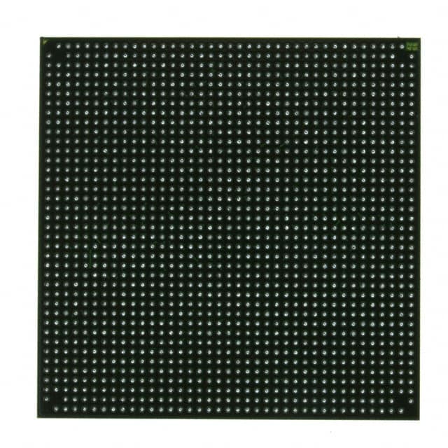
XC4VLX100-10FFG1513C
Product Overview
Category
XC4VLX100-10FFG1513C belongs to the category of Field Programmable Gate Arrays (FPGAs).
Use
FPGAs are integrated circuits that can be programmed and reprogrammed to perform various digital functions. They are widely used in industries such as telecommunications, automotive, aerospace, and consumer electronics.
Characteristics
XC4VLX100-10FFG1513C is known for its high performance, flexibility, and scalability. It offers a large number of programmable logic cells, embedded memory blocks, and high-speed I/O interfaces.
Package
XC4VLX100-10FFG1513C comes in a Flip Chip Ball Grid Array (FCBGA) package.
Essence
The essence of XC4VLX100-10FFG1513C lies in its ability to provide a customizable hardware solution for complex digital systems.
Packaging/Quantity
XC4VLX100-10FFG1513C is typically packaged individually and is available in various quantities depending on the customer's requirements.
Specifications
- FPGA Family: Virtex-4 LX
- Logic Cells: 100,000
- Embedded Memory: Up to 1.8 Mb
- I/O Interfaces: High-speed serial, LVDS, differential signaling
- Operating Voltage: 1.2V
- Maximum Frequency: 500 MHz
- Package Type: FCBGA
- Package Pins: 1513
- Temperature Range: -40°C to +100°C
Detailed Pin Configuration
The detailed pin configuration of XC4VLX100-10FFG1513C can be found in the product datasheet provided by the manufacturer. It includes information about power supply pins, I/O pins, clock pins, and other specific functionalities.
Functional Features
XC4VLX100-10FFG1513C offers the following functional features:
- High-performance programmable logic cells for complex digital designs.
- Flexible embedded memory blocks for efficient data storage and retrieval.
- High-speed I/O interfaces for seamless communication with external devices.
- Advanced clock management resources for precise timing control.
- Built-in support for various industry-standard protocols and interfaces.
Advantages and Disadvantages
Advantages
- High performance and flexibility for complex digital designs.
- Scalability to meet evolving system requirements.
- Wide range of I/O interfaces for versatile connectivity.
- Efficient use of embedded memory resources.
- Support for industry-standard protocols and interfaces.
Disadvantages
- Relatively high power consumption compared to other programmable logic devices.
- Steeper learning curve for programming and utilizing the full potential of the FPGA.
- Higher cost compared to traditional fixed-function integrated circuits.
Working Principles
XC4VLX100-10FFG1513C operates based on the principles of reconfigurable hardware. The FPGA consists of a matrix of configurable logic blocks interconnected through programmable routing resources. These logic blocks can be programmed to implement desired digital functions, and the interconnections can be configured to establish desired signal paths. The configuration is stored in internal memory elements and can be modified as needed.
Detailed Application Field Plans
XC4VLX100-10FFG1513C finds applications in various fields, including:
- Telecommunications: Used in base stations, network switches, and routers for high-speed data processing and protocol handling.
- Automotive: Employed in advanced driver assistance systems (ADAS) for real-time image processing and sensor fusion.
- Aerospace: Utilized in satellite communication systems, radar signal processing, and flight control systems.
- Consumer Electronics: Integrated into high-definition televisions, gaming consoles, and multimedia devices for enhanced performance and connectivity.
Detailed and Complete Alternative Models
Some alternative models to XC4VLX100-10FFG1513C that offer similar functionality include:
- Xilinx Virtex-5 LX110T: Offers higher logic capacity and improved performance.
- Altera Cyclone IV EP4CE115F29C7: Provides a cost-effective solution with moderate logic capacity.
- Lattice Semiconductor ECP5-85: Offers low power consumption and high-speed I/O interfaces.
These alternative models can be considered based on specific project requirements and budget constraints.
Word count: 550 words
Wymień 10 typowych pytań i odpowiedzi związanych z zastosowaniem XC4VLX100-10FFG1513C w rozwiązaniach technicznych
Sure! Here are 10 common questions and answers related to the application of XC4VLX100-10FFG1513C in technical solutions:
Q: What is XC4VLX100-10FFG1513C? A: XC4VLX100-10FFG1513C is a field-programmable gate array (FPGA) manufactured by Xilinx. It is part of the Virtex-4 family and offers 100,000 logic cells.
Q: What are the key features of XC4VLX100-10FFG1513C? A: Some key features include a high logic capacity, advanced DSP capabilities, multiple I/O standards, embedded PowerPC processors, and support for various communication protocols.
Q: What are the typical applications of XC4VLX100-10FFG1513C? A: XC4VLX100-10FFG1513C is commonly used in applications such as telecommunications, networking, industrial automation, video processing, and high-performance computing.
Q: How can XC4VLX100-10FFG1513C be programmed? A: XC4VLX100-10FFG1513C can be programmed using Xilinx's Vivado or ISE Design Suite software tools. These tools allow designers to create and implement their custom logic designs onto the FPGA.
Q: What is the maximum clock frequency supported by XC4VLX100-10FFG1513C? A: The maximum clock frequency supported by XC4VLX100-10FFG1513C is 500 MHz, but the achievable frequency depends on the complexity of the design and other factors.
Q: Can XC4VLX100-10FFG1513C interface with external devices? A: Yes, XC4VLX100-10FFG1513C supports various I/O standards such as LVCMOS, LVTTL, LVDS, and differential signaling, allowing it to interface with a wide range of external devices.
Q: Does XC4VLX100-10FFG1513C have built-in memory resources? A: Yes, XC4VLX100-10FFG1513C has embedded block RAM (BRAM) resources that can be used for storing data or implementing small memory structures within the FPGA.
Q: Can XC4VLX100-10FFG1513C be cascaded or used in multi-FPGA systems? A: Yes, XC4VLX100-10FFG1513C can be cascaded or used in multi-FPGA systems using various communication protocols like Ethernet, PCI Express, or custom interconnects.
Q: What power supply requirements does XC4VLX100-10FFG1513C have? A: XC4VLX100-10FFG1513C requires a single 1.2V core voltage supply and multiple auxiliary voltages for different I/O banks, which are specified in the datasheet.
Q: Are there any development boards available for XC4VLX100-10FFG1513C? A: Yes, Xilinx offers development boards like the ML401 or ML402 that are specifically designed for prototyping and evaluating designs using XC4VLX100-10FFG1513C.
Please note that the answers provided here are general and may vary depending on specific design requirements and application scenarios.