

Szczegóły produktu można znaleźć w specyfikacjach.
XC2VP7-7FFG896C
Product Overview
Category
XC2VP7-7FFG896C belongs to the category of Field Programmable Gate Arrays (FPGAs).
Use
This FPGA is primarily used for digital logic design and implementation in various electronic systems.
Characteristics
- High-performance programmable logic device
- Offers flexibility and reconfigurability
- Provides high-speed processing capabilities
- Supports complex digital designs
- Enables rapid prototyping and development
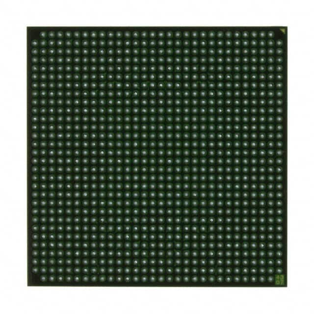
Package
XC2VP7-7FFG896C comes in a Fine-Pitch Ball Grid Array (FBGA) package.
Essence
The essence of XC2VP7-7FFG896C lies in its ability to provide a customizable hardware platform for implementing digital circuits.
Packaging/Quantity
Each package of XC2VP7-7FFG896C contains one FPGA unit.
Specifications
- Device Type: Field Programmable Gate Array
- Family: Virtex-II Pro
- Logic Cells: 6,912
- Slices: 1,152
- Flip-Flops: 4,608
- Block RAM: 648 Kb
- Maximum Frequency: 400 MHz
- I/O Pins: 896
- Operating Voltage: 1.5V
- Package Type: FBGA
- Package Pins: 896
- Temperature Range: -40°C to +100°C
Detailed Pin Configuration
The detailed pin configuration of XC2VP7-7FFG896C can be found in the product datasheet provided by the manufacturer.
Functional Features
XC2VP7-7FFG896C offers the following functional features:
- Configurable logic blocks
- Digital signal processing capabilities
- Embedded PowerPC processor cores
- High-speed serial transceivers
- On-chip memory resources
- Clock management resources
- Various I/O standards and interfaces
Advantages and Disadvantages
Advantages
- High-performance and flexibility
- Reconfigurable for different applications
- Supports complex digital designs
- Enables rapid prototyping and development
- Offers a wide range of I/O options
Disadvantages
- Relatively high power consumption
- Requires expertise in FPGA programming
- Limited availability of alternative models
Working Principles
XC2VP7-7FFG896C operates based on the principles of reconfigurable hardware. It consists of configurable logic blocks, interconnect resources, and various other components that can be programmed to implement desired digital circuits. The FPGA is configured using a bitstream file generated by a design tool, which defines the functionality and interconnections of the circuit.
Detailed Application Field Plans
XC2VP7-7FFG896C finds applications in various fields, including:
- Communications: Used in wireless base stations, network routers, and communication infrastructure equipment.
- Aerospace and Defense: Employed in radar systems, avionics, and military communication devices.
- Industrial Automation: Utilized in control systems, robotics, and factory automation.
- Medical Electronics: Applied in medical imaging devices, patient monitoring systems, and diagnostic equipment.
- Automotive: Used in advanced driver-assistance systems (ADAS), infotainment systems, and engine control units.
Alternative Models
While XC2VP7-7FFG896C is a highly capable FPGA, there are alternative models available from different manufacturers. Some notable alternatives include:
- Altera Cyclone V GX: Offers similar performance and features with a different architecture.
- Lattice ECP5: Provides a low-power option with competitive capabilities.
- Xilinx Spartan-6: A cost-effective FPGA suitable for less demanding applications.
These alternative models can be considered based on specific project requirements and budget constraints.
In conclusion, XC2VP7-7FFG896C is a high-performance FPGA that offers flexibility, reconfigurability, and rapid prototyping capabilities. It finds applications in various fields and provides a customizable hardware platform for implementing complex digital designs. While it has advantages such as high performance and flexibility, it also has disadvantages like high power consumption and limited availability of alternative models.
Wymień 10 typowych pytań i odpowiedzi związanych z zastosowaniem XC2VP7-7FFG896C w rozwiązaniach technicznych
Sure! Here are 10 common questions and answers related to the application of XC2VP7-7FFG896C in technical solutions:
Q: What is XC2VP7-7FFG896C? A: XC2VP7-7FFG896C is a field-programmable gate array (FPGA) manufactured by Xilinx.
Q: What are the key features of XC2VP7-7FFG896C? A: Some key features include 7,680 logic cells, 576 Kbits of block RAM, 8 Digital Clock Managers (DCMs), and support for various I/O standards.
Q: What applications can XC2VP7-7FFG896C be used for? A: XC2VP7-7FFG896C can be used in a wide range of applications such as telecommunications, industrial automation, image processing, and high-performance computing.
Q: How does XC2VP7-7FFG896C differ from other FPGAs? A: XC2VP7-7FFG896C offers a balance between logic capacity, performance, and power consumption, making it suitable for many mid-range applications.
Q: What programming languages can be used with XC2VP7-7FFG896C? A: XC2VP7-7FFG896C can be programmed using hardware description languages (HDLs) such as VHDL or Verilog.
Q: Can XC2VP7-7FFG896C be reprogrammed after deployment? A: Yes, XC2VP7-7FFG896C is a reprogrammable FPGA, allowing for flexibility and updates in the field.
Q: What development tools are available for XC2VP7-7FFG896C? A: Xilinx provides software tools like Vivado Design Suite, which includes synthesis, simulation, and implementation tools for designing with XC2VP7-7FFG896C.
Q: What is the power consumption of XC2VP7-7FFG896C? A: The power consumption of XC2VP7-7FFG896C depends on the specific design and operating conditions but typically ranges from a few watts to tens of watts.
Q: Can XC2VP7-7FFG896C interface with other components or devices? A: Yes, XC2VP7-7FFG896C supports various I/O standards and can interface with other components or devices such as memory, sensors, or communication interfaces.
Q: Are there any known limitations or considerations when using XC2VP7-7FFG896C? A: Some considerations include the need for proper cooling due to power dissipation, understanding the timing constraints of the design, and ensuring compatibility with other system components.
Please note that these answers are general and may vary depending on the specific requirements and context of your technical solution.