

Szczegóły produktu można znaleźć w specyfikacjach.
XC2VP7-6FFG896I
Product Overview
Category
XC2VP7-6FFG896I belongs to the category of Field Programmable Gate Arrays (FPGAs).
Use
This product is primarily used in digital logic circuits for various applications such as telecommunications, automotive, aerospace, and consumer electronics.
Characteristics
- High-performance FPGA with advanced features
- Large number of programmable logic cells
- Flexible I/O options
- High-speed interfaces
- Low power consumption
Package
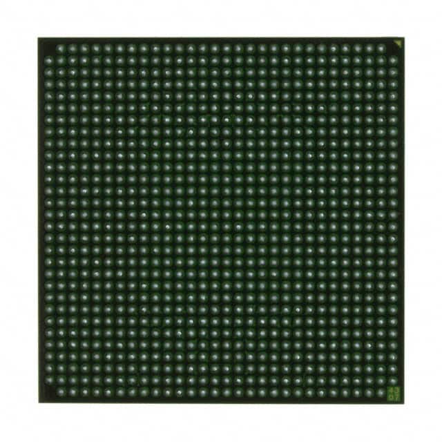
XC2VP7-6FFG896I is available in a Fine-Pitch Ball Grid Array (FBGA) package.
Essence
The essence of XC2VP7-6FFG896I lies in its ability to provide reconfigurable hardware that can be programmed to perform specific functions based on user requirements.
Packaging/Quantity
This product is typically sold individually and comes in a standard packaging quantity of one unit per package.
Specifications
- Device Type: FPGA
- Family: Virtex-II Pro
- Logic Cells: 7,680
- Number of I/Os: 576
- Operating Voltage: 1.5V
- Maximum Frequency: 400 MHz
- Package Type: FBGA
- Package Pins: 896
- Temperature Range: -40°C to +100°C
Detailed Pin Configuration
The detailed pin configuration of XC2VP7-6FFG896I can be found in the product datasheet provided by the manufacturer.
Functional Features
- High-density programmable logic cells for complex designs
- Built-in multipliers and memory blocks for efficient implementation of arithmetic operations
- Configurable I/O standards for interfacing with different devices
- On-chip clock management resources for precise timing control
- Support for various communication protocols and high-speed interfaces
Advantages and Disadvantages
Advantages
- Versatile and flexible design options
- High-performance capabilities
- Low power consumption compared to traditional ASICs
- Shorter development time due to reprogrammability
- Cost-effective for low to medium volume production
Disadvantages
- Limited resources compared to custom-designed ASICs
- Higher cost per unit compared to mass-produced integrated circuits
- Relatively higher power consumption compared to dedicated hardware solutions
Working Principles
XC2VP7-6FFG896I operates based on the principles of FPGA technology. It consists of a matrix of programmable logic cells interconnected through configurable routing resources. The device can be programmed using Hardware Description Languages (HDL) such as VHDL or Verilog, which define the desired functionality of the circuit. Upon programming, the FPGA configuration is loaded into the device, enabling it to perform the specified operations.
Detailed Application Field Plans
XC2VP7-6FFG896I finds applications in various fields, including:
- Telecommunications: Used in base stations, network switches, and routers for high-speed data processing and protocol handling.
- Automotive: Employed in advanced driver assistance systems (ADAS), engine control units (ECUs), and infotainment systems for enhanced performance and connectivity.
- Aerospace: Utilized in satellite communication systems, avionics, and radar systems for reliable and efficient signal processing.
- Consumer Electronics: Integrated into high-definition televisions, gaming consoles, and multimedia devices for multimedia processing and interface control.
Detailed and Complete Alternative Models
- XC2VP30-6FFG896I: A lower-density variant with 30,000 logic cells and similar features.
- XC2VP50-6FFG896I: A mid-range option with 50,000 logic cells and expanded I/O capabilities.
- XC2VP100-6FFG896I: A higher-density model with 100,000 logic cells and increased performance.
These alternative models provide a range of options to suit different project requirements.
Word count: 550 words
Wymień 10 typowych pytań i odpowiedzi związanych z zastosowaniem XC2VP7-6FFG896I w rozwiązaniach technicznych
Sure! Here are 10 common questions and answers related to the application of XC2VP7-6FFG896I in technical solutions:
Question: What is XC2VP7-6FFG896I?
- Answer: XC2VP7-6FFG896I is a field-programmable gate array (FPGA) manufactured by Xilinx.Question: What are the key features of XC2VP7-6FFG896I?
- Answer: Some key features include 7,680 logic cells, 576 Kbits of block RAM, 16 DSP slices, and support for various I/O standards.Question: What applications can XC2VP7-6FFG896I be used for?
- Answer: XC2VP7-6FFG896I can be used in a wide range of applications such as telecommunications, industrial automation, image processing, and high-performance computing.Question: What is the maximum operating frequency of XC2VP7-6FFG896I?
- Answer: The maximum operating frequency of XC2VP7-6FFG896I is typically around 400 MHz.Question: Can XC2VP7-6FFG896I be reprogrammed after deployment?
- Answer: Yes, XC2VP7-6FFG896I is a field-programmable device, which means it can be reprogrammed even after it has been deployed in a system.Question: What development tools are available for programming XC2VP7-6FFG896I?
- Answer: Xilinx provides software tools like Vivado and ISE Design Suite that can be used to program and configure XC2VP7-6FFG896I.Question: What is the power consumption of XC2VP7-6FFG896I?
- Answer: The power consumption of XC2VP7-6FFG896I depends on the specific design and operating conditions, but it typically ranges from a few watts to tens of watts.Question: Can XC2VP7-6FFG896I interface with other components or devices?
- Answer: Yes, XC2VP7-6FFG896I supports various I/O standards and can interface with other components or devices such as memory, sensors, and communication interfaces.Question: Are there any limitations or considerations when using XC2VP7-6FFG896I?
- Answer: Some considerations include the available resources (logic cells, RAM, etc.), power requirements, and the need for proper cooling and thermal management.Question: Where can I find more information about XC2VP7-6FFG896I?
- Answer: You can refer to Xilinx's official documentation, datasheets, application notes, and online forums for more detailed information about XC2VP7-6FFG896I.
Please note that the answers provided here are general and may vary depending on specific use cases and requirements.