

Szczegóły produktu można znaleźć w specyfikacjach.
XC2C128-7VQG100I
Product Overview
Category
XC2C128-7VQG100I belongs to the category of programmable logic devices (PLDs).
Use
This product is commonly used in digital circuit design and implementation. It provides a flexible and customizable solution for various applications.
Characteristics
- Programmable: The XC2C128-7VQG100I can be programmed to perform specific functions based on the user's requirements.
- High-density: This PLD offers a high number of logic elements, allowing for complex designs.
- Low power consumption: The device is designed to operate efficiently with minimal power consumption.
- Fast operation: The XC2C128-7VQG100I offers high-speed performance, enabling quick processing of digital signals.
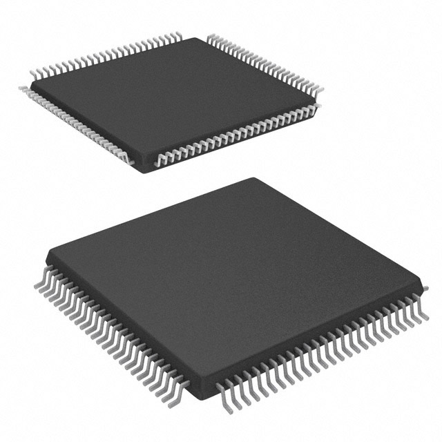
Package
The XC2C128-7VQG100I is available in a VQG100 package.
Essence
The essence of XC2C128-7VQG100I lies in its ability to provide reconfigurable logic functionality, allowing users to implement custom digital circuits without the need for dedicated hardware.
Packaging/Quantity
This product is typically packaged individually and is available in various quantities depending on the manufacturer's specifications.
Specifications
- Logic Elements: 128
- Maximum Frequency: 100 MHz
- I/O Pins: 100
- Operating Voltage: 3.3V
- Operating Temperature Range: -40°C to 85°C
- Configuration Memory: 128Kbits
Detailed Pin Configuration
The XC2C128-7VQG100I has a total of 100 I/O pins. These pins are used for input and output connections to external devices. The pin configuration is as follows:
(Pin Number) - (Pin Name) 1 - IO0 2 - IO1 3 - IO2 ... 100 - IO99
Functional Features
- Reconfigurable Logic: The XC2C128-7VQG100I allows users to modify the logic functions according to their specific requirements.
- Flexible I/O: The device offers a high number of I/O pins, enabling easy interfacing with external devices.
- Fast Operation: With a maximum frequency of 100 MHz, this PLD ensures efficient processing of digital signals.
Advantages and Disadvantages
Advantages
- Flexibility: The reconfigurable nature of XC2C128-7VQG100I allows for versatile application in various digital circuit designs.
- Cost-effective: By eliminating the need for dedicated hardware, this PLD reduces overall costs.
- High-density: The device provides a large number of logic elements, enabling complex designs.
Disadvantages
- Learning Curve: Utilizing the full potential of this PLD may require a learning curve for users unfamiliar with programmable logic devices.
- Limited Resources: The XC2C128-7VQG100I has a finite number of logic elements, which may restrict the complexity of certain designs.
Working Principles
The XC2C128-7VQG100I operates based on the principles of field-programmable gate arrays (FPGAs). It consists of configurable logic blocks (CLBs) interconnected through programmable interconnects. These CLBs can be programmed to implement desired logic functions, allowing for the creation of custom digital circuits.
Detailed Application Field Plans
XC2C128-7VQG100I finds applications in various fields, including: 1. Communications: Used in the design of communication protocols and signal processing algorithms. 2. Industrial Automation: Employed in control systems and data acquisition modules. 3. Consumer Electronics: Integrated into multimedia devices, gaming consoles, and home automation systems. 4. Automotive: Utilized in automotive electronics for engine control, driver assistance systems, and infotainment.
Detailed and Complete Alternative Models
- XC2C256-7VQG100I: Similar to XC2C128-7VQG100I but with double the logic elements.
- XC2C384-7VQG100I: Offers higher logic density compared to XC2C128-7VQG100I.
- XC2C512-7VQG100I: Provides the highest logic capacity among the alternative models.
These alternative models offer increased capabilities and can be considered based on the specific requirements of the application.
Word count: 550 words
Wymień 10 typowych pytań i odpowiedzi związanych z zastosowaniem XC2C128-7VQG100I w rozwiązaniach technicznych
Sure! Here are 10 common questions and answers related to the application of XC2C128-7VQG100I in technical solutions:
Question: What is XC2C128-7VQG100I?
- Answer: XC2C128-7VQG100I is a specific model of CoolRunner-II CPLD (Complex Programmable Logic Device) manufactured by Xilinx.Question: What is the purpose of XC2C128-7VQG100I in technical solutions?
- Answer: XC2C128-7VQG100I is used for implementing digital logic functions in various electronic systems, such as control systems, communication devices, and embedded systems.Question: What are the key features of XC2C128-7VQG100I?
- Answer: Some key features of XC2C128-7VQG100I include 128 macrocells, 128 flip-flops, 4 global clock lines, and support for up to 128 I/O pins.Question: How is XC2C128-7VQG100I programmed?
- Answer: XC2C128-7VQG100I can be programmed using Xilinx's programming tools, such as iMPACT or Vivado, which allow users to configure the device with their desired logic functions.Question: Can XC2C128-7VQG100I be reprogrammed?
- Answer: Yes, XC2C128-7VQG100I is a reprogrammable device, meaning that its configuration can be changed multiple times to adapt to different requirements.Question: What are some advantages of using XC2C128-7VQG100I in technical solutions?
- Answer: Some advantages include its low power consumption, small form factor, high reliability, and ability to implement complex logic functions in a single device.Question: What are the voltage requirements for XC2C128-7VQG100I?
- Answer: XC2C128-7VQG100I operates at a supply voltage of 3.3V, which is commonly used in many electronic systems.Question: Can XC2C128-7VQG100I interface with other components or devices?
- Answer: Yes, XC2C128-7VQG100I can interface with other components or devices through its I/O pins, allowing it to communicate with external sensors, memory modules, or other digital devices.Question: Are there any limitations or considerations when using XC2C128-7VQG100I?
- Answer: Some considerations include the limited number of I/O pins and macrocells available, as well as the need for proper signal integrity and timing analysis during design.Question: Where can I find more information about XC2C128-7VQG100I and its applications?
- Answer: You can refer to Xilinx's official documentation, datasheets, application notes, and online forums for more detailed information and examples of XC2C128-7VQG100I's applications in technical solutions.