

Szczegóły produktu można znaleźć w specyfikacjach.
Encyclopedia Entry: 74VHC540FT
Product Overview
Category
The 74VHC540FT belongs to the category of integrated circuits (ICs) and specifically falls under the family of VHC series logic gates.
Use
This IC is commonly used in digital electronic circuits for signal amplification, buffering, and level shifting purposes. It serves as a voltage-controlled buffer with 3-state outputs.
Characteristics
- High-speed operation: The 74VHC540FT offers fast switching times, making it suitable for applications requiring quick response.
- Low power consumption: This IC is designed to minimize power consumption, making it energy-efficient.
- Wide operating voltage range: It can operate within a wide voltage range, typically between 2V and 5.5V.
- 3-state outputs: The 74VHC540FT features three-state outputs, allowing multiple devices to share a common bus without interference.
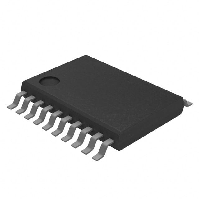
Package
The 74VHC540FT is available in a small-sized surface mount package, such as TSSOP-20 or SSOP-20. These packages provide ease of integration into various circuit designs.
Essence
The essence of the 74VHC540FT lies in its ability to amplify and buffer digital signals while maintaining compatibility with different voltage levels. It ensures reliable signal transmission and efficient communication between different components of a digital system.
Packaging/Quantity
Typically, the 74VHC540FT is supplied in reels or tubes, containing a specific quantity of ICs per package. The exact packaging and quantity may vary depending on the manufacturer and supplier.
Specifications
- Supply Voltage Range: 2V to 5.5V
- Input Voltage Range: 0V to VCC
- Output Voltage Range: 0V to VCC
- Maximum Operating Frequency: XX MHz
- Number of Inputs: 8
- Number of Outputs: 8
- Logic Family: VHC
- Logic Type: Buffer/Driver, Non-Inverting
- Output Type: 3-State
- Package Type: TSSOP-20, SSOP-20
Detailed Pin Configuration
The 74VHC540FT has a total of 20 pins, which are assigned specific functions as follows:
- Pin 1: Input A1
- Pin 2: Input A2
- Pin 3: Input A3
- Pin 4: Input A4
- Pin 5: Input A5
- Pin 6: Input A6
- Pin 7: Input A7
- Pin 8: Input A8
- Pin 9: GND (Ground)
- Pin 10: Output Y1
- Pin 11: Output Y2
- Pin 12: Output Y3
- Pin 13: Output Y4
- Pin 14: Output Y5
- Pin 15: Output Y6
- Pin 16: Output Y7
- Pin 17: Output Y8
- Pin 18: OE (Output Enable)
- Pin 19: VCC (Supply Voltage)
- Pin 20: NC (No Connection)
Functional Features
- Signal Amplification: The 74VHC540FT amplifies digital signals received at its inputs to ensure reliable transmission to the outputs.
- Level Shifting: It can shift the voltage levels of input signals to match the requirements of downstream components.
- 3-State Outputs: The IC features 3-state outputs, allowing for high impedance when disabled, preventing signal interference on shared buses.
- High-Speed Operation: With fast switching times, it enables efficient data transfer in time-critical applications.
Advantages and Disadvantages
Advantages
- High-speed operation facilitates quick response in time-sensitive applications.
- Low power consumption ensures energy efficiency.
- Wide operating voltage range allows compatibility with various systems.
- 3-state outputs enable efficient bus sharing without interference.
Disadvantages
- Limited number of inputs and outputs may restrict its use in complex circuits requiring more connections.
- Sensitivity to electrostatic discharge (ESD) requires proper handling during installation and usage.
Working Principles
The 74VHC540FT operates based on the principles of CMOS (Complementary Metal-Oxide-Semiconductor) technology. It utilizes a combination of NMOS (N-channel Metal-Oxide-Semiconductor) and PMOS (P-channel Metal-Oxide-Semiconductor) transistors to achieve its functionality. When enabled, the IC amplifies and buffers digital signals received at its inputs, ensuring accurate transmission to the outputs. The 3-state outputs allow for high impedance when disabled, preventing signal interference on shared buses.
Detailed Application Field Plans
The 74VHC540FT finds application in various digital
Wymień 10 typowych pytań i odpowiedzi związanych z zastosowaniem 74VHC540FT w rozwiązaniach technicznych
Sure! Here are 10 common questions and answers related to the application of 74VHC540FT in technical solutions:
Q: What is the 74VHC540FT? A: The 74VHC540FT is a high-speed octal buffer/line driver integrated circuit (IC) that can be used for signal buffering and driving applications.
Q: What is the operating voltage range of the 74VHC540FT? A: The 74VHC540FT operates within a voltage range of 2.0V to 5.5V.
Q: How many channels does the 74VHC540FT have? A: The 74VHC540FT has 8 channels, making it suitable for applications requiring multiple buffered outputs.
Q: What is the maximum output current of the 74VHC540FT? A: The 74VHC540FT can source or sink up to 8mA of current per channel.
Q: Can the 74VHC540FT handle bidirectional data flow? A: Yes, the 74VHC540FT supports bidirectional data flow, allowing it to be used for both input and output buffering.
Q: Does the 74VHC540FT have any built-in protection features? A: No, the 74VHC540FT does not have built-in protection features. External measures may be required to protect against overvoltage or ESD events.
Q: What is the typical propagation delay of the 74VHC540FT? A: The typical propagation delay of the 74VHC540FT is around 4.5ns, making it suitable for high-speed applications.
Q: Can the 74VHC540FT be used in both CMOS and TTL logic systems? A: Yes, the 74VHC540FT is compatible with both CMOS and TTL logic levels, allowing it to be used in a wide range of systems.
Q: What is the package type of the 74VHC540FT? A: The 74VHC540FT is available in a TSSOP (Thin Shrink Small Outline Package) package.
Q: Are there any recommended decoupling capacitors for the 74VHC540FT? A: It is generally recommended to use a 0.1μF ceramic capacitor placed close to the power supply pins of the IC to provide decoupling and stability.
Please note that these answers are general and may vary depending on specific application requirements and datasheet specifications.