

Szczegóły produktu można znaleźć w specyfikacjach.
XC6501A3017R-G
Product Overview
Category
XC6501A3017R-G belongs to the category of voltage regulators.
Use
It is commonly used in electronic circuits to regulate and stabilize the voltage supplied to various components.
Characteristics
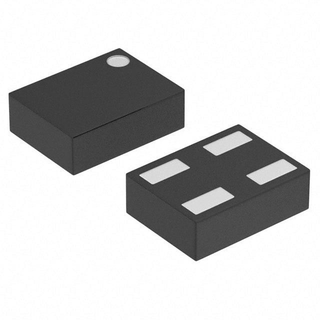
- Package: XC6501A3017R-G is available in a small surface-mount package.
- Essence: It is a low dropout voltage regulator with high accuracy and low power consumption.
- Packaging/Quantity: The product is typically packaged in reels or tubes, with varying quantities depending on the supplier.
Specifications
The specifications for XC6501A3017R-G are as follows:
- Input Voltage Range: 2.5V - 6.0V
- Output Voltage: 1.7V
- Output Current: 150mA
- Dropout Voltage: 200mV (typical)
- Quiescent Current: 30μA (typical)
- Operating Temperature Range: -40°C to +85°C
Pin Configuration
The detailed pin configuration for XC6501A3017R-G is as follows:
Pin 1: VIN (Input Voltage)
Pin 2: GND (Ground)
Pin 3: VOUT (Output Voltage)
Functional Features
XC6501A3017R-G offers the following functional features:
- Low dropout voltage: Provides stable output even when the input voltage is close to the desired output voltage.
- High accuracy: Ensures precise regulation of the output voltage.
- Low power consumption: Minimizes energy wastage during operation.
Advantages and Disadvantages
Advantages: - Small package size allows for space-saving designs. - Wide input voltage range provides flexibility in various applications. - Low quiescent current enables energy-efficient operation.
Disadvantages: - Limited output current may not be suitable for high-power applications. - Dropout voltage may affect the efficiency in certain scenarios.
Working Principles
XC6501A3017R-G operates based on the principle of a linear voltage regulator. It uses a pass transistor to regulate the output voltage by adjusting the resistance between the input and output terminals. This ensures that the output voltage remains constant, even when the input voltage fluctuates.
Detailed Application Field Plans
XC6501A3017R-G finds applications in various electronic devices and systems, including but not limited to: - Battery-powered devices - Portable consumer electronics - IoT devices - Automotive electronics - Industrial control systems
Detailed and Complete Alternative Models
Some alternative models that can be considered as alternatives to XC6501A3017R-G are: - LM1117-1.8: A low dropout voltage regulator with an output voltage of 1.8V. - LT1763: A high-performance, low dropout voltage regulator with adjustable output voltage. - TPS7A4700: An ultra-low noise, low dropout voltage regulator suitable for sensitive applications.
These alternative models offer similar functionalities and can be chosen based on specific requirements and design constraints.
Word count: 311 words
Wymień 10 typowych pytań i odpowiedzi związanych z zastosowaniem XC6501A3017R-G w rozwiązaniach technicznych
Sure! Here are 10 common questions and answers related to the application of XC6501A3017R-G in technical solutions:
Q1: What is XC6501A3017R-G? A1: XC6501A3017R-G is a specific model of voltage regulator IC (integrated circuit) manufactured by Torex Semiconductor. It is designed to provide stable and regulated voltage output for various electronic applications.
Q2: What is the input voltage range of XC6501A3017R-G? A2: The input voltage range of XC6501A3017R-G is typically between 2.5V and 6.0V.
Q3: What is the output voltage of XC6501A3017R-G? A3: The output voltage of XC6501A3017R-G is fixed at 3.3V.
Q4: What is the maximum output current of XC6501A3017R-G? A4: The maximum output current of XC6501A3017R-G is 150mA.
Q5: Is XC6501A3017R-G suitable for battery-powered applications? A5: Yes, XC6501A3017R-G is suitable for battery-powered applications as it has a low dropout voltage and operates efficiently even with lower input voltages.
Q6: Can XC6501A3017R-G be used in automotive applications? A6: Yes, XC6501A3017R-G can be used in automotive applications as it meets the necessary requirements for automotive electronics, such as temperature range and reliability.
Q7: Does XC6501A3017R-G have built-in protection features? A7: Yes, XC6501A3017R-G includes built-in protection features like overcurrent protection, thermal shutdown, and reverse current protection.
Q8: Can XC6501A3017R-G be used in space-constrained designs? A8: Yes, XC6501A3017R-G is available in a small SOT-23 package, making it suitable for space-constrained designs.
Q9: What is the operating temperature range of XC6501A3017R-G? A9: The operating temperature range of XC6501A3017R-G is typically between -40°C and +85°C.
Q10: Are there any application notes or reference designs available for XC6501A3017R-G? A10: Yes, Torex Semiconductor provides application notes and reference designs for XC6501A3017R-G, which can help in implementing the IC effectively in various technical solutions.
Please note that the answers provided here are general and may vary depending on specific datasheet specifications and application requirements.