

Szczegóły produktu można znaleźć w specyfikacjach.
TPS610982DSER
Product Overview
Category
The TPS610982DSER belongs to the category of integrated circuits (ICs) and specifically falls under the voltage regulators - switching regulators classification.
Use
This product is primarily used for boosting or stepping up voltage levels in various electronic devices and systems. It provides a regulated output voltage that is higher than the input voltage.
Characteristics
- High efficiency: The TPS610982DSER offers high conversion efficiency, minimizing power losses during voltage conversion.
- Wide input voltage range: It can accept a wide range of input voltages, making it suitable for diverse applications.
- Adjustable output voltage: The output voltage can be adjusted according to the specific requirements of the application.
- Low quiescent current: The device consumes minimal current when not actively regulating the voltage, conserving power.
Package
The TPS610982DSER is available in a small outline package (SOP) with a compact footprint. This package ensures ease of integration into various circuit designs.
Essence
The essence of the TPS610982DSER lies in its ability to efficiently boost input voltages to higher levels while maintaining stable and regulated output voltages.
Packaging/Quantity
The TPS610982DSER is typically packaged in reels or tubes, containing a specified quantity of ICs per package. The exact packaging and quantity may vary depending on the manufacturer's specifications.
Specifications
- Input Voltage Range: 2.7V to 12V
- Output Voltage Range: 3.3V to 15V
- Maximum Output Current: 1A
- Switching Frequency: 1.2MHz
- Operating Temperature Range: -40°C to +85°C
- Package Type: SOP-8
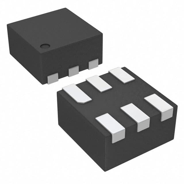
Detailed Pin Configuration
The TPS610982DSER features an SOP-8 package with the following pin configuration:
- VIN: Input voltage pin
- EN: Enable pin (active high)
- FB: Feedback pin for output voltage regulation
- GND: Ground reference pin
- SW: Switching node pin
- NC: No connection
- NC: No connection
- VOUT: Output voltage pin
Functional Features
- Wide input voltage range: The TPS610982DSER can accept input voltages ranging from 2.7V to 12V, allowing flexibility in various applications.
- High efficiency: With its efficient switching regulator design, the device achieves high conversion efficiency, reducing power losses.
- Adjustable output voltage: The output voltage can be adjusted using external resistors, enabling customization based on specific requirements.
- Protection features: The IC incorporates protection mechanisms such as overcurrent protection and thermal shutdown, ensuring safe operation.
Advantages and Disadvantages
Advantages
- High conversion efficiency leads to reduced power consumption.
- Wide input voltage range allows for versatile application scenarios.
- Adjustable output voltage provides flexibility in meeting different system requirements.
- Compact package size facilitates easy integration into circuit designs.
Disadvantages
- Limited maximum output current of 1A may not be suitable for high-power applications.
- SOP-8 package may have limitations in terms of heat dissipation compared to larger packages.
Working Principles
The TPS610982DSER operates as a step-up (boost) voltage regulator. It utilizes a switching regulator topology to efficiently convert the input voltage to a higher regulated output voltage. The internal control circuitry adjusts the duty cycle of the switching transistor to maintain the desired output voltage level.
When the input voltage is applied, the control circuitry monitors the feedback voltage and adjusts the duty cycle accordingly. This regulates the output voltage within the specified range. The switching frequency of 1.2MHz ensures fast response and stable operation.
Detailed Application Field Plans
The TPS610982DSER finds applications in various electronic devices and systems, including but not limited to:
- Battery-powered portable devices: It can be used to boost the battery voltage to power components requiring higher voltages.
- LED lighting systems: The IC can provide the necessary voltage levels for driving LEDs efficiently.
- Industrial automation: It can be employed in control systems that require regulated high-voltage supplies.
- Automotive electronics: The TPS610982DSER can be utilized in automotive applications where voltage boosting is required.
Detailed and Complete Alternative Models
- TPS610981DSER: Similar to TPS610982DSER, but with a lower maximum output current of 500mA.
- TPS610983DSER: Similar to TPS610982DSER, but with a higher maximum output current of 1.5A.
- TPS61165DSGR: A step-up voltage regulator with an integrated boost converter and adjustable output voltage.
These alternative models offer similar functionality and can be considered based on specific application
Wymień 10 typowych pytań i odpowiedzi związanych z zastosowaniem TPS610982DSER w rozwiązaniach technicznych
Sure! Here are 10 common questions and answers related to the application of TPS610982DSER in technical solutions:
Q: What is the TPS610982DSER? A: The TPS610982DSER is a boost converter integrated circuit (IC) that provides a regulated output voltage from a lower input voltage.
Q: What is the input voltage range of the TPS610982DSER? A: The TPS610982DSER has an input voltage range of 0.9V to 5.5V.
Q: What is the output voltage range of the TPS610982DSER? A: The TPS610982DSER can provide an output voltage range from 1.8V to 5.25V.
Q: What is the maximum output current of the TPS610982DSER? A: The TPS610982DSER can deliver a maximum output current of 1A.
Q: Can the TPS610982DSER operate in low-power mode? A: Yes, the TPS610982DSER features a low-power mode that reduces the quiescent current for improved efficiency in light-load conditions.
Q: Does the TPS610982DSER have built-in protection features? A: Yes, the TPS610982DSER includes overvoltage protection, undervoltage lockout, and thermal shutdown protection.
Q: What type of package does the TPS610982DSER come in? A: The TPS610982DSER is available in a small 2mm x 2mm WSON-8 package.
Q: Can the TPS610982DSER be used in battery-powered applications? A: Yes, the TPS610982DSER is suitable for battery-powered applications due to its low input voltage range and efficient operation.
Q: What are some typical applications of the TPS610982DSER? A: The TPS610982DSER can be used in portable devices, IoT applications, wearables, and other low-power systems that require a regulated output voltage.
Q: Is there any evaluation board available for the TPS610982DSER? A: Yes, Texas Instruments provides an evaluation module (TPS610982EVM-001) that allows users to test and evaluate the performance of the TPS610982DSER in their applications.
Please note that these answers are general and may vary depending on the specific requirements and use cases. It's always recommended to refer to the datasheet and application notes provided by the manufacturer for detailed information.