

Szczegóły produktu można znaleźć w specyfikacjach.
TPS61040DRVR
Product Overview
Category
The TPS61040DRVR belongs to the category of integrated circuits (ICs) and specifically falls under the voltage regulators - switching regulators classification.
Use
This product is primarily used for boosting or stepping up voltages in various electronic applications. It is commonly employed in portable devices, battery-powered systems, and other low-power applications where efficient voltage conversion is required.
Characteristics
- High efficiency: The TPS61040DRVR offers high efficiency conversion, minimizing power losses during voltage boosting.
- Wide input voltage range: It can operate with input voltages ranging from 0.9V to 6V, making it suitable for a wide range of power sources.
- Adjustable output voltage: The output voltage can be adjusted using external resistors, allowing flexibility in meeting specific application requirements.
- Low quiescent current: The device features low quiescent current consumption, ensuring minimal power drain when not actively boosting voltage.
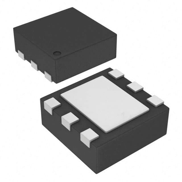
Package
The TPS61040DRVR comes in a small outline package (DRV) with a size of 6-pin SOT-23. This compact package enables easy integration into space-constrained designs.
Essence
The essence of the TPS61040DRVR lies in its ability to efficiently boost input voltages to higher levels, providing a stable and regulated output voltage for various electronic devices.
Packaging/Quantity
The TPS61040DRVR is typically available in tape and reel packaging, with a quantity of 3000 units per reel.
Specifications
- Input Voltage Range: 0.9V to 6V
- Output Voltage Range: Adjustable (based on external resistors)
- Switching Frequency: 1.2MHz
- Maximum Output Current: 400mA
- Quiescent Current: 30µA
- Operating Temperature Range: -40°C to 85°C
Detailed Pin Configuration
The TPS61040DRVR has the following pin configuration:
- VIN: Input voltage pin
- GND: Ground reference pin
- FB: Feedback pin for output voltage regulation
- EN: Enable pin for device operation control
- SW: Switching node pin
- VOUT: Output voltage pin
Functional Features
- High Efficiency: The TPS61040DRVR offers high efficiency conversion, reducing power losses and maximizing battery life in portable devices.
- Wide Input Voltage Range: It can accept a wide range of input voltages, making it compatible with various power sources.
- Adjustable Output Voltage: The output voltage can be easily adjusted using external resistors, allowing customization for different applications.
- Low Quiescent Current: The device consumes minimal current when not actively boosting voltage, minimizing power drain.
Advantages and Disadvantages
Advantages
- High efficiency conversion
- Wide input voltage range
- Adjustable output voltage
- Compact package size
- Low quiescent current consumption
Disadvantages
- Limited maximum output current (400mA)
Working Principles
The TPS61040DRVR operates as a step-up (boost) voltage regulator. It utilizes a switching topology to efficiently convert lower input voltages to higher output voltages. The internal control circuitry adjusts the duty cycle of the switching transistor to regulate the output voltage based on the feedback received from the FB pin.
Detailed Application Field Plans
The TPS61040DRVR finds application in various fields, including but not limited to: - Portable electronic devices (e.g., smartphones, tablets, portable media players) - Battery-powered systems (e.g., wireless sensors, IoT devices) - Low-power applications requiring voltage boosting
Detailed and Complete Alternative Models
Some alternative models that offer similar functionality to the TPS61040DRVR include: - TPS61041DRVR - TPS61042DRVR - TPS61043DRVR
These models share comparable specifications and pin configurations, providing alternative options for voltage boosting applications.
Word count: 530 words
Wymień 10 typowych pytań i odpowiedzi związanych z zastosowaniem TPS61040DRVR w rozwiązaniach technicznych
Sure! Here are 10 common questions and answers related to the application of TPS61040DRVR in technical solutions:
Q: What is TPS61040DRVR? A: TPS61040DRVR is a boost converter IC (integrated circuit) designed for applications requiring a regulated output voltage higher than the input voltage.
Q: What is the input voltage range of TPS61040DRVR? A: The input voltage range of TPS61040DRVR is typically between 0.9V and 6V.
Q: What is the output voltage range of TPS61040DRVR? A: The output voltage range of TPS61040DRVR can be adjusted from 1.8V to 5.5V using external resistors.
Q: What is the maximum output current of TPS61040DRVR? A: The maximum output current of TPS61040DRVR is 400mA.
Q: Can TPS61040DRVR operate in low-power mode? A: Yes, TPS61040DRVR has a low-power mode that reduces the quiescent current to minimize power consumption during light load conditions.
Q: Does TPS61040DRVR have built-in protection features? A: Yes, TPS61040DRVR includes over-temperature protection, over-current protection, and under-voltage lockout to ensure safe operation.
Q: Can TPS61040DRVR be used in battery-powered applications? A: Yes, TPS61040DRVR is suitable for battery-powered applications as it can efficiently boost the input voltage to a higher level.
Q: Is TPS61040DRVR compatible with both analog and digital loads? A: Yes, TPS61040DRVR can be used with both analog and digital loads, making it versatile for various applications.
Q: What is the typical efficiency of TPS61040DRVR? A: The typical efficiency of TPS61040DRVR is around 90%, depending on the input and output voltage levels.
Q: Can TPS61040DRVR be used in automotive applications? A: Yes, TPS61040DRVR is automotive-grade and can be used in automotive applications that require a boost converter.
Please note that these answers are general and may vary depending on specific application requirements and conditions.