

Szczegóły produktu można znaleźć w specyfikacjach.
TLV4111IDGNG4
Product Overview
Category: Integrated Circuits (ICs)
Use: The TLV4111IDGNG4 is a high-speed operational amplifier designed for use in various applications, including audio amplification, signal conditioning, and sensor interfacing.
Characteristics: - High bandwidth and slew rate for accurate signal reproduction - Low input bias current for minimal signal distortion - Rail-to-rail input and output voltage range for maximum dynamic range - Low noise and distortion for high-fidelity audio applications
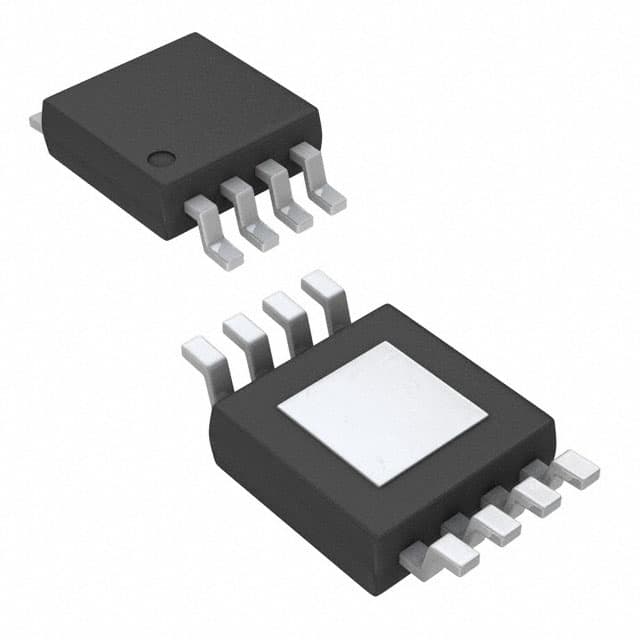
Package: The TLV4111IDGNG4 is available in an 8-pin VSSOP package, which offers a compact form factor and easy integration into circuit designs.
Essence: The TLV4111IDGNG4 is a versatile operational amplifier that provides high-performance signal amplification and conditioning capabilities.
Packaging/Quantity: The TLV4111IDGNG4 is typically sold in reels or tubes, with a quantity of 2500 units per reel/tube.
Specifications
- Supply Voltage Range: 2.7V to 5.5V
- Input Offset Voltage: ±1.5mV (maximum)
- Input Bias Current: ±1pA (maximum)
- Gain Bandwidth Product: 50MHz
- Slew Rate: 25V/µs
- Input/Output Voltage Range: Rail-to-Rail
- Operating Temperature Range: -40°C to +125°C
Detailed Pin Configuration
The TLV4111IDGNG4 features the following pin configuration:
- OUT: Output pin
- IN-: Inverting input pin
- IN+: Non-inverting input pin
- V-: Negative power supply pin
- NC: No connection
- V+: Positive power supply pin
- NC: No connection
- GND: Ground pin
Functional Features
- High-speed amplification: The TLV4111IDGNG4 offers a high gain bandwidth product and slew rate, enabling accurate reproduction of fast-changing signals.
- Low distortion: With low input bias current and rail-to-rail voltage range, the amplifier minimizes signal distortion and ensures faithful signal representation.
- Wide supply voltage range: The TLV4111IDGNG4 operates from 2.7V to 5.5V, making it suitable for various power supply configurations.
- Small form factor: The VSSOP package allows for space-efficient integration into circuit designs.
Advantages and Disadvantages
Advantages: - High-speed performance - Low distortion and noise - Wide supply voltage range - Compact package size
Disadvantages: - Limited availability in certain regions - Higher cost compared to some alternative models
Working Principles
The TLV4111IDGNG4 is based on a differential amplifier configuration, where the difference between the non-inverting and inverting inputs is amplified. It utilizes internal compensation techniques to achieve stability and maintain performance over a wide range of operating conditions.
Detailed Application Field Plans
The TLV4111IDGNG4 finds applications in various fields, including: - Audio amplification systems - Signal conditioning circuits - Sensor interface circuits - Data acquisition systems - Active filters
Detailed and Complete Alternative Models
- TLV4110IDGNG4: Similar specifications and features, but with a different pin configuration (inverting and non-inverting inputs are swapped).
- TLV4112IDGNG4: Dual operational amplifier with similar characteristics, suitable for applications requiring multiple amplification channels.
- LMV321IDBVR: Lower-cost alternative with slightly reduced performance specifications.
These alternative models provide flexibility in selecting the most suitable operational amplifier for specific application requirements.
Word count: 409 words
Wymień 10 typowych pytań i odpowiedzi związanych z zastosowaniem TLV4111IDGNG4 w rozwiązaniach technicznych
Sure! Here are 10 common questions and answers related to the application of TLV4111IDGNG4 in technical solutions:
Q1: What is TLV4111IDGNG4? A1: TLV4111IDGNG4 is a low-power, precision operational amplifier designed for general-purpose applications.
Q2: What is the supply voltage range for TLV4111IDGNG4? A2: The supply voltage range for TLV4111IDGNG4 is typically between 2.7V and 5.5V.
Q3: What is the input offset voltage of TLV4111IDGNG4? A3: The input offset voltage of TLV4111IDGNG4 is typically 0.5mV.
Q4: What is the input bias current of TLV4111IDGNG4? A4: The input bias current of TLV4111IDGNG4 is typically 1pA.
Q5: What is the gain bandwidth product of TLV4111IDGNG4? A5: The gain bandwidth product of TLV4111IDGNG4 is typically 10MHz.
Q6: Can TLV4111IDGNG4 operate in single-supply mode? A6: Yes, TLV4111IDGNG4 can operate in both single-supply and dual-supply modes.
Q7: What is the maximum output current of TLV4111IDGNG4? A7: The maximum output current of TLV4111IDGNG4 is typically 40mA.
Q8: Is TLV4111IDGNG4 suitable for low-power applications? A8: Yes, TLV4111IDGNG4 is designed for low-power applications, making it suitable for battery-powered devices.
Q9: Can TLV4111IDGNG4 be used in precision measurement applications? A9: Yes, TLV4111IDGNG4 offers low input offset voltage and low input bias current, making it suitable for precision measurement applications.
Q10: What is the temperature range for TLV4111IDGNG4? A10: The temperature range for TLV4111IDGNG4 is typically -40°C to 125°C.
Please note that the answers provided here are general and may vary depending on specific datasheet specifications.