

Szczegóły produktu można znaleźć w specyfikacjach.
SN74AHCT374DGVR
Basic Information Overview
- Category: Integrated Circuit (IC)
- Use: Flip-Flop
- Characteristics: High-speed, low-power, 8-bit D-type flip-flop with 3-state outputs
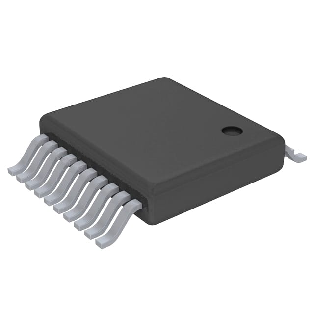
- Package: VSSOP (Very Small Outline Package)
- Essence: Sequential logic device used for storing and transferring data in digital systems
- Packaging/Quantity: Tape and Reel, 2500 units per reel
Specifications
- Supply Voltage Range: 4.5V to 5.5V
- Input Voltage Range: 0V to VCC
- Output Voltage Range: 0V to VCC
- Operating Temperature Range: -40°C to +85°C
- Output Drive Capability: ±24mA at 3.3V
- Propagation Delay Time: 6.5ns (typical)
Detailed Pin Configuration
- GND: Ground
- CP: Clock Pulse Input
- D0-D7: Data Inputs
- OE: Output Enable Input
- Q0-Q7: Flip-Flop Outputs
- VCC: Power Supply
Functional Features
- 8-bit D-type flip-flop with 3-state outputs
- Positive-edge triggered clock input
- Asynchronous master reset input
- 3-state outputs for bus-oriented applications
- Low power consumption
- High-speed operation
Advantages
- Compact VSSOP package allows for space-saving designs
- Wide operating voltage range ensures compatibility with various systems
- High-speed operation enables efficient data transfer
- Low power consumption reduces energy requirements
- 3-state outputs facilitate bus-oriented applications
Disadvantages
- Limited output drive capability may not be suitable for high-current applications
- Not suitable for use in extreme temperature conditions
Working Principles
The SN74AHCT374DGVR is a positive-edge triggered D-type flip-flop. It stores and transfers data based on the clock input signal. When the clock pulse rises from low to high, the data present at the inputs (D0-D7) is latched and transferred to the corresponding outputs (Q0-Q7). The asynchronous master reset input (OE) allows for resetting the flip-flop to a known state. The 3-state outputs enable multiple devices to share a common bus.
Detailed Application Field Plans
The SN74AHCT374DGVR is widely used in digital systems where sequential data storage and transfer are required. Some specific application fields include: 1. Microcontrollers and microprocessors 2. Data communication systems 3. Memory modules 4. Industrial automation 5. Automotive electronics
Detailed and Complete Alternative Models
- SN74HC374N: Similar functionality, but operates at a higher voltage range (2V to 6V)
- CD4013BE: Dual D-type flip-flop with similar characteristics, but in a different package (PDIP)
Note: This is not an exhaustive list of alternative models. Please refer to the manufacturer's datasheet for a complete list of alternatives.
In conclusion, the SN74AHCT374DGVR is a high-speed, low-power 8-bit D-type flip-flop with 3-state outputs. Its compact VSSOP package, wide operating voltage range, and efficient data transfer make it suitable for various digital applications. However, its limited output drive capability and temperature limitations should be considered when selecting this IC for specific projects.
Wymień 10 typowych pytań i odpowiedzi związanych z zastosowaniem SN74AHCT374DGVR w rozwiązaniach technicznych
Sure! Here are 10 common questions and answers related to the application of SN74AHCT374DGVR:
Q: What is SN74AHCT374DGVR? A: SN74AHCT374DGVR is a type of integrated circuit (IC) known as a flip-flop, specifically a D-type flip-flop with 3-state outputs.
Q: What is the purpose of SN74AHCT374DGVR? A: SN74AHCT374DGVR is used for storing and transferring binary data in digital circuits. It can be used for various applications such as data storage, synchronization, and signal buffering.
Q: What voltage levels does SN74AHCT374DGVR support? A: SN74AHCT374DGVR supports a wide range of voltage levels, typically from 2V to 5.5V.
Q: How many flip-flops are there in SN74AHCT374DGVR? A: SN74AHCT374DGVR contains 8 individual flip-flops, each capable of storing one bit of data.
Q: Can SN74AHCT374DGVR be used in both synchronous and asynchronous applications? A: Yes, SN74AHCT374DGVR can be used in both synchronous and asynchronous applications, depending on the design requirements.
Q: What is the maximum clock frequency supported by SN74AHCT374DGVR? A: SN74AHCT374DGVR can operate at high clock frequencies, typically up to 100 MHz.
Q: Does SN74AHCT374DGVR have any special power requirements? A: SN74AHCT374DGVR operates on a single power supply voltage, typically between 2V and 5.5V, making it compatible with a wide range of digital systems.
Q: Can SN74AHCT374DGVR drive external loads directly? A: Yes, SN74AHCT374DGVR has 3-state outputs that can drive external loads directly, making it suitable for driving other digital circuits or devices.
Q: Is SN74AHCT374DGVR sensitive to noise or voltage fluctuations? A: SN74AHCT374DGVR is designed to be relatively immune to noise and voltage fluctuations, thanks to its built-in Schmitt trigger inputs.
Q: Are there any specific precautions to consider when using SN74AHCT374DGVR? A: It is important to ensure proper decoupling capacitors are used near the power supply pins of SN74AHCT374DGVR to minimize noise and voltage spikes. Additionally, care should be taken to avoid exceeding the maximum voltage and current ratings specified in the datasheet.
Please note that these answers are general and may vary depending on the specific application and design considerations. Always refer to the datasheet and consult with an expert for accurate information.