

Szczegóły produktu można znaleźć w specyfikacjach.
SN74AHC139DGVR
Product Overview
- Category: Integrated Circuit (IC)
- Use: Decoder/Demultiplexer
- Characteristics:
- High-speed CMOS technology
- Low power consumption
- Wide operating voltage range
- Multiple package options
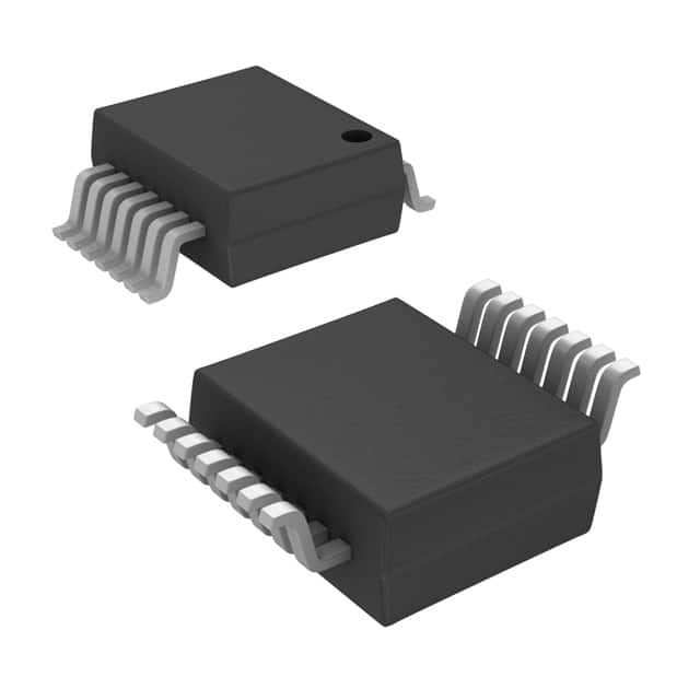
- Package: VSSOP-16
- Essence: Dual 2-to-4 line decoder/demultiplexer
- Packaging/Quantity: Tape and Reel, 2500 units per reel
Specifications
- Supply Voltage Range: 2V to 5.5V
- Input Voltage Range: 0V to VCC
- Output Voltage Range: 0V to VCC
- Operating Temperature Range: -40°C to +85°C
- Propagation Delay Time: 6 ns (typical)
- Maximum Quiescent Current: 1 μA
Detailed Pin Configuration
The SN74AHC139DGVR has a VSSOP-16 package with the following pin configuration:
__    __
   A1 |1  \__/ 16| VCC
   A0 |2        15| Y0
   E1 |3        14| Y1
   E2 |4        13| Y2
   Y3 |5        12| Y3
   GND|6        11| Y4
   Y7 |7        10| Y5
   Y6 |8         9| Y6
       ‾‾    ‾‾
Functional Features
- Dual 2-to-4 line decoder/demultiplexer
- Decodes two binary inputs into four mutually exclusive outputs
- Enables easy selection of one output from multiple inputs
- High-speed operation suitable for various applications
- Low power consumption makes it energy-efficient
- Wide operating voltage range allows compatibility with different systems
Advantages and Disadvantages
Advantages: - High-speed CMOS technology ensures fast operation - Low power consumption extends battery life in portable devices - Wide operating voltage range provides flexibility in system design - Multiple package options cater to different application requirements
Disadvantages: - Limited number of output lines (4) may not be sufficient for complex applications - Propagation delay time (6 ns) may impact timing-sensitive circuits
Working Principles
The SN74AHC139DGVR is a decoder/demultiplexer IC that takes two binary inputs, A1 and A0, and decodes them into four mutually exclusive outputs, Y0 to Y3. The enable pins, E1 and E2, control the operation of the decoder/demultiplexer. When both enable pins are high, all outputs are disabled.
The IC operates on high-speed CMOS technology, allowing for fast decoding and demultiplexing of input signals. It has a wide operating voltage range, making it compatible with various systems. The low power consumption of the IC makes it suitable for energy-efficient applications.
Detailed Application Field Plans
The SN74AHC139DGVR can be used in various applications, including:
- Address decoding in microcontrollers and microprocessors
- Data routing and selection in multiplexers
- Memory address decoding in RAM and ROM modules
- Signal demultiplexing in communication systems
- Control signal generation in digital logic circuits
Detailed and Complete Alternative Models
- 74HC139: Similar dual 2-to-4 line decoder/demultiplexer from NXP Semiconductors
- CD74HC139: Dual 2-to-4 line decoder/demultiplexer from Texas Instruments
- MC74HC139: High-speed CMOS dual 2-to-4 line decoder/demultiplexer from ON Semiconductor
These alternative models offer similar functionality and can be used as replacements for the SN74AHC139DGVR in various applications.
Word count: 446 words
Wymień 10 typowych pytań i odpowiedzi związanych z zastosowaniem SN74AHC139DGVR w rozwiązaniach technicznych
Sure! Here are 10 common questions and answers related to the application of SN74AHC139DGVR in technical solutions:
Q: What is the SN74AHC139DGVR? A: The SN74AHC139DGVR is a dual 2-to-4 line decoder/demultiplexer integrated circuit (IC) that can be used in various digital logic applications.
Q: What is the operating voltage range of SN74AHC139DGVR? A: The operating voltage range of SN74AHC139DGVR is typically between 2V and 5.5V.
Q: How many inputs does SN74AHC139DGVR have? A: SN74AHC139DGVR has two 2-inputs, A0 and A1, which are used for selecting the output lines.
Q: How many output lines does SN74AHC139DGVR have? A: SN74AHC139DGVR has four output lines, Y0, Y1, Y2, and Y3.
Q: Can SN74AHC139DGVR be used as a demultiplexer? A: Yes, SN74AHC139DGVR can be used as a demultiplexer by connecting the appropriate input lines and using the outputs accordingly.
Q: What is the maximum output current of SN74AHC139DGVR? A: The maximum output current of SN74AHC139DGVR is typically 8mA.
Q: Can SN74AHC139DGVR be cascaded to increase the number of output lines? A: Yes, multiple SN74AHC139DGVR ICs can be cascaded together to increase the number of output lines.
Q: What is the propagation delay of SN74AHC139DGVR? A: The propagation delay of SN74AHC139DGVR is typically around 6ns.
Q: Can SN74AHC139DGVR be used in high-speed applications? A: Yes, SN74AHC139DGVR is designed for high-speed operation and can be used in various high-frequency applications.
Q: What are some typical applications of SN74AHC139DGVR? A: Some typical applications of SN74AHC139DGVR include address decoding, data routing, memory selection, and general-purpose digital logic circuits.
Please note that the answers provided here are general and may vary depending on specific datasheet specifications and application requirements.