Szczegóły produktu można znaleźć w specyfikacjach.

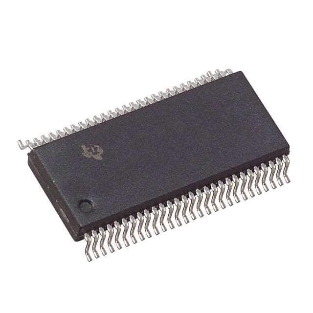
SN74ABT18640DLRG4
Product Overview
- Category: Integrated Circuit (IC)
- Use: Logic Device
- Characteristics: High-speed, low-power, 18-bit universal bus transceiver
- Package: 56-pin TSSOP (Thin Shrink Small Outline Package)
- Essence: Transceiver IC for bidirectional data transfer between buses
- Packaging/Quantity: Tape and Reel, 2500 units per reel
Specifications
- Technology: Advanced BiCMOS
- Supply Voltage: 2.3V to 3.6V
- Input/Output Compatibility: TTL (Transistor-Transistor Logic) and CMOS (Complementary Metal-Oxide-Semiconductor)
- Operating Temperature Range: -40°C to +85°C
- Output Drive Capability: ±24mA
- Propagation Delay: 3.5ns (Max)
- Output Skew: 250ps (Max)
Detailed Pin Configuration
The SN74ABT18640DLRG4 has a total of 56 pins. The pin configuration is as follows:
- OE (Output Enable) A1
- A1
- B1
- C1
- D1
- E1
- F1
- G1
- H1
- I1
- J1
- K1
- L1
- M1
- N1
- O1
- P1
- VCC (Positive Power Supply)
- GND (Ground)
- OE (Output Enable) B1
- A2
- B2
- C2
- D2
- E2
- F2
- G2
- H2
- I2
- J2
- K2
- L2
- M2
- N2
- O2
- P2
- OE (Output Enable) A2
- A3
- B3
- C3
- D3
- E3
- F3
- G3
- H3
- I3
- J3
- K3
- L3
- M3
- N3
- O3
- P3
- OE (Output Enable) B2
- VCC
- GND
Functional Features
- Bidirectional data transfer between two independent buses
- Non-inverting outputs for both A and B buses
- Output enable control for each bus
- 18-bit wide data path
- High-speed operation with low power consumption
- TTL and CMOS compatible inputs and outputs
- Schmitt-trigger input for noise immunity
Advantages and Disadvantages
Advantages: - High-speed operation allows for efficient data transfer - Low power consumption helps in reducing overall system energy usage - Compatibility with both TTL and CMOS devices ensures versatility - Schmitt-trigger input provides noise immunity, enhancing signal integrity
Disadvantages: - Limited to 18-bit data path, may not be suitable for applications requiring larger data widths - Availability of alternative models with additional features or different specifications may limit its competitiveness in certain scenarios
Working Principles
The SN74ABT18640DLRG4 is designed to facilitate bidirectional data transfer between two independent buses. It operates by receiving data from one bus and transmitting it to the other bus, while also allowing data flow in the opposite direction. The output enable control feature allows the user to enable or disable the data transfer on each bus independently.
Detailed Application Field Plans
The SN74ABT18640DLRG4 can be used in various applications, including but not limited to: - Data communication systems - Networking equipment - Industrial automation - Automotive electronics - Consumer electronics
Detailed and Complete Alternative Models
- SN74ABT18640DLR: Similar to SN74ABT18640DLRG4, but without the "G4" suffix indicating RoHS compliance.
- SN74ABT18640DLRQ1: Automotive-grade version of SN74ABT18640DLR, designed for harsh operating conditions.
- SN74ABT18640DLRSM: Enhanced version with extended temperature range (-55°C to +125°C) for extreme environments.
These alternative models offer different features or specifications to cater to specific application requirements.
Word count: 489 words
Wymień 10 typowych pytań i odpowiedzi związanych z zastosowaniem SN74ABT18640DLRG4 w rozwiązaniach technicznych
Sure! Here are 10 common questions and answers related to the application of SN74ABT18640DLRG4:
Q: What is the SN74ABT18640DLRG4? A: The SN74ABT18640DLRG4 is a 64-bit bus transceiver with 3-state outputs, designed for high-speed digital systems.
Q: What is the maximum operating voltage for this device? A: The SN74ABT18640DLRG4 has a maximum operating voltage of 3.6V.
Q: What is the typical propagation delay of this transceiver? A: The typical propagation delay of the SN74ABT18640DLRG4 is 5.8 ns.
Q: Can I use this transceiver in a bidirectional data bus application? A: Yes, the SN74ABT18640DLRG4 is suitable for bidirectional data bus applications.
Q: Does this device support hot insertion? A: Yes, the SN74ABT18640DLRG4 supports hot insertion, allowing it to be inserted or removed from a live circuit.
Q: What is the maximum output current that this transceiver can drive? A: The SN74ABT18640DLRG4 can drive up to 32 mA of output current.
Q: Is this device compatible with TTL logic levels? A: Yes, the SN74ABT18640DLRG4 is compatible with both TTL and CMOS logic levels.
Q: Can I use this transceiver in a high-speed data communication system? A: Yes, the SN74ABT18640DLRG4 is designed for high-speed digital systems and can be used in high-speed data communication applications.
Q: Does this device have built-in ESD protection? A: Yes, the SN74ABT18640DLRG4 has built-in ESD protection to safeguard against electrostatic discharge.
Q: What is the package type for this transceiver? A: The SN74ABT18640DLRG4 is available in a 56-pin TSSOP (Thin Shrink Small Outline Package) package.
Please note that these answers are general and may vary depending on the specific application and requirements. It's always recommended to refer to the datasheet and consult with the manufacturer for detailed information.

