

Szczegóły produktu można znaleźć w specyfikacjach.
SCANSTA112SMX/NOPB
Product Overview
- Category: Integrated Circuit (IC)
- Use: Signal Conditioning and Data Acquisition
- Characteristics: High-performance, low-power, compact size
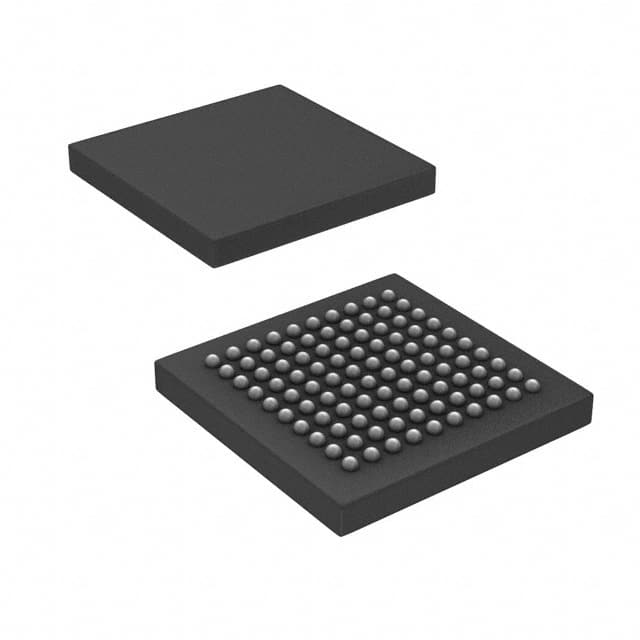
- Package: Surface Mount Technology (SMT)
- Essence: Signal conditioning and data acquisition IC
- Packaging/Quantity: Tape and Reel, 2500 units per reel
Specifications
- Operating Voltage: 3.3V
- Operating Temperature Range: -40°C to +85°C
- Input Channels: 12 differential or 24 single-ended
- Resolution: 16-bit
- Sampling Rate: Up to 100 kSPS (kilo samples per second)
- Interface: SPI (Serial Peripheral Interface)
- Power Consumption: Low power consumption, typically 5mW
- Package Dimensions: 4mm x 4mm
Detailed Pin Configuration
The SCANSTA112SMX/NOPB has the following pin configuration:
- VDD: Power supply voltage
- GND: Ground
- SCLK: Serial Clock input for SPI communication
- SDI: Serial Data Input for SPI communication
- SDO: Serial Data Output for SPI communication
- CS: Chip Select input for SPI communication
- REF: Reference voltage input
- AIN0-AIN11: Analog Input Channels
- DOUT: Digital Output
- DIN: Digital Input
- CLK: Clock input
- RESET: Reset input
Functional Features
- High-resolution ADC (Analog-to-Digital Converter) for accurate signal conversion
- Flexible input channel configuration for various applications
- Low power consumption for energy-efficient operation
- Compact size allows for space-saving designs
- SPI interface enables easy integration with microcontrollers and other devices
Advantages and Disadvantages
Advantages
- High-performance signal conditioning and data acquisition capabilities
- Wide operating temperature range for versatile usage scenarios
- Compact package size suitable for space-constrained applications
- Low power consumption for energy-efficient designs
- Flexible input channel configuration for diverse measurement requirements
Disadvantages
- Limited to SPI interface, may not be compatible with all communication protocols
- Requires external reference voltage for accurate analog-to-digital conversion
- May require additional components for complete system integration
Working Principles
The SCANSTA112SMX/NOPB is designed to condition and acquire analog signals. It utilizes a high-resolution ADC to convert analog signals into digital data. The SPI interface allows for easy communication with microcontrollers or other devices. The IC operates at a low power consumption level, making it suitable for battery-powered applications. By configuring the input channels, users can select between differential or single-ended measurements based on their specific needs.
Detailed Application Field Plans
The SCANSTA112SMX/NOPB finds applications in various fields, including:
- Industrial Automation: Signal conditioning and data acquisition in control systems, monitoring equipment, and process automation.
- Medical Devices: Accurate measurement and acquisition of vital signs, patient monitoring, and diagnostic equipment.
- Test and Measurement: Precise data acquisition in laboratory instruments, data loggers, and test equipment.
- Energy Management: Monitoring and control of energy consumption in smart grid systems, renewable energy systems, and building automation.
- Automotive: Sensor signal conditioning and data acquisition in automotive electronics, vehicle diagnostics, and safety systems.
Detailed and Complete Alternative Models
- AD7124-8: 16-bit, 8-channel, low-power ADC with SPI interface.
- MCP3421: 18-bit, 1-channel, low-power ADC with I2C interface.
- MAX11100: 16-bit, 12-channel, low-power ADC with SPI interface.
These alternative models offer similar functionality and can be considered as alternatives to the SCANSTA112SMX/NOPB based on specific requirements and system compatibility.
Word count: 450 words
Wymień 10 typowych pytań i odpowiedzi związanych z zastosowaniem SCANSTA112SMX/NOPB w rozwiązaniach technicznych
What is the operating temperature range of SCANSTA112SMX/NOPB?
- The operating temperature range of SCANSTA112SMX/NOPB is -40°C to 125°C.What is the typical supply voltage for SCANSTA112SMX/NOPB?
- The typical supply voltage for SCANSTA112SMX/NOPB is 3.3V.Can SCANSTA112SMX/NOPB be used in automotive applications?
- Yes, SCANSTA112SMX/NOPB is suitable for automotive applications.What is the maximum data rate supported by SCANSTA112SMX/NOPB?
- SCANSTA112SMX/NOPB supports a maximum data rate of 100 Mbps.Is SCANSTA112SMX/NOPB RoHS compliant?
- Yes, SCANSTA112SMX/NOPB is RoHS compliant.Does SCANSTA112SMX/NOPB support hot-swapping capability?
- Yes, SCANSTA112SMX/NOPB supports hot-swapping capability.What is the package type of SCANSTA112SMX/NOPB?
- SCANSTA112SMX/NOPB comes in a 48-pin LQFP package.Can SCANSTA112SMX/NOPB be used in industrial control systems?
- Yes, SCANSTA112SMX/NOPB is suitable for use in industrial control systems.What is the power consumption of SCANSTA112SMX/NOPB in standby mode?
- The power consumption of SCANSTA112SMX/NOPB in standby mode is typically 10mW.Is there a recommended layout for PCB design when using SCANSTA112SMX/NOPB?
- Yes, Texas Instruments provides a recommended PCB layout in the datasheet for SCANSTA112SMX/NOPB.