

Szczegóły produktu można znaleźć w specyfikacjach.
LM25115SDX
Product Overview
Category: Integrated Circuit (IC)
Use: LM25115SDX is a high-performance synchronous buck regulator designed for use in various power management applications.
Characteristics: - High efficiency - Wide input voltage range - Adjustable output voltage - Current mode control - Overcurrent protection - Thermal shutdown protection
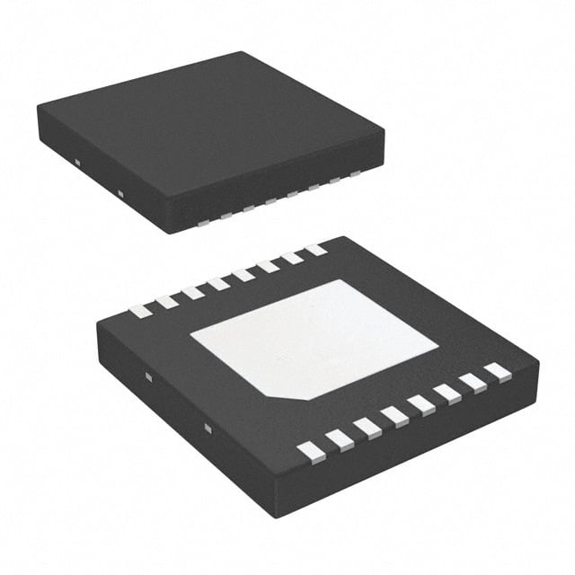
Package: LM25115SDX is available in a small outline package (SOP) with 8 pins.
Essence: The essence of LM25115SDX lies in its ability to efficiently regulate voltage in power management applications, ensuring stable and reliable power supply.
Packaging/Quantity: LM25115SDX is typically sold in reels containing 2500 units per reel.
Specifications
- Input Voltage Range: 4.5V to 42V
- Output Voltage Range: 0.8V to 20V
- Maximum Output Current: 3A
- Switching Frequency: Up to 1MHz
- Operating Temperature Range: -40°C to +125°C
Pin Configuration
The LM25115SDX features the following pin configuration:
- VIN: Input voltage pin
- GND: Ground pin
- FB: Feedback pin for output voltage regulation
- EN: Enable pin for turning the regulator on/off
- SS/TR: Soft-start/Tracking pin for controlling startup behavior
- PGND: Power ground pin
- SW: Switch node pin for connecting the inductor and power switch
- VOUT: Output voltage pin
Functional Features
- High Efficiency: LM25115SDX offers high efficiency due to its synchronous rectification and low RDS(ON) MOSFETs.
- Adjustable Output Voltage: The output voltage can be easily adjusted using external resistors.
- Current Mode Control: The regulator utilizes current mode control for improved stability and transient response.
- Overcurrent Protection: LM25115SDX incorporates overcurrent protection to safeguard against excessive load currents.
- Thermal Shutdown Protection: The device includes thermal shutdown protection to prevent damage from excessive temperature.
Advantages and Disadvantages
Advantages: - Wide input voltage range allows for versatile applications - High efficiency results in reduced power dissipation - Adjustable output voltage provides flexibility - Current mode control enhances stability and response - Overcurrent and thermal shutdown protection ensure safety
Disadvantages: - Limited maximum output current of 3A may not be suitable for high-power applications - SOP package may limit heat dissipation capabilities in certain scenarios
Working Principles
LM25115SDX operates as a synchronous buck regulator, converting a higher input voltage to a lower output voltage. It utilizes pulse width modulation (PWM) to control the duty cycle of the internal power switch, regulating the output voltage. The feedback pin (FB) monitors the output voltage and adjusts the duty cycle accordingly. The regulator also employs current mode control to enhance stability and transient response.
Detailed Application Field Plans
LM25115SDX finds applications in various fields, including but not limited to: 1. Industrial automation systems 2. Automotive electronics 3. Telecommunications equipment 4. Power supplies for consumer electronics 5. LED lighting systems
Alternative Models
For those seeking alternatives to LM25115SDX, the following models provide similar functionality: 1. LM25116SDX 2. LM25117SDX 3. LM25118SDX
These alternative models offer comparable specifications and features, allowing users to choose the most suitable option for their specific requirements.
Word count: 511 words
Wymień 10 typowych pytań i odpowiedzi związanych z zastosowaniem LM25115SDX w rozwiązaniach technicznych
Sure! Here are 10 common questions and answers related to the application of LM25115SDX in technical solutions:
Q: What is LM25115SDX? A: LM25115SDX is a synchronous buck regulator IC (integrated circuit) designed for high-efficiency power conversion applications.
Q: What is the input voltage range of LM25115SDX? A: The input voltage range of LM25115SDX is typically between 4.5V and 42V.
Q: What is the output voltage range of LM25115SDX? A: The output voltage range of LM25115SDX can be adjusted from 0.8V to 90% of the input voltage.
Q: What is the maximum output current of LM25115SDX? A: The maximum output current of LM25115SDX is 3A.
Q: What is the efficiency of LM25115SDX? A: The efficiency of LM25115SDX can reach up to 95%, depending on the input and output conditions.
Q: Can LM25115SDX operate in a wide temperature range? A: Yes, LM25115SDX has a wide operating temperature range of -40°C to +125°C.
Q: Does LM25115SDX have built-in protection features? A: Yes, LM25115SDX includes various protection features such as thermal shutdown, overcurrent protection, and undervoltage lockout.
Q: Can LM25115SDX be used in automotive applications? A: Yes, LM25115SDX is suitable for automotive applications as it meets the AEC-Q100 Grade 1 qualification standards.
Q: What is the package type of LM25115SDX? A: LM25115SDX is available in a small 8-pin WSON (Wide Small Outline No-Lead) package.
Q: Are there any evaluation boards or reference designs available for LM25115SDX? A: Yes, Texas Instruments provides evaluation boards and reference designs to help users quickly prototype and implement LM25115SDX in their applications.
Please note that these answers are general and may vary depending on the specific application and requirements.