

Szczegóły produktu można znaleźć w specyfikacjach.
DS90LV804TSQ/NOPB
Product Overview
- Category: Integrated Circuit
- Use: High-speed LVDS Serializer/Deserializer
- Characteristics: Low-voltage differential signaling, high-speed data transmission, compact package, reliable performance
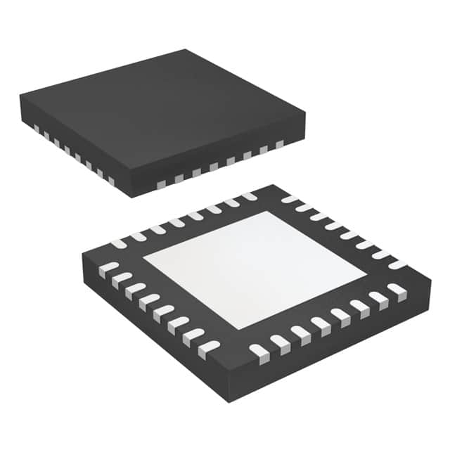
- Package: 48-pin TSSOP (Thin Shrink Small Outline Package)
- Essence: DS90LV804TSQ/NOPB is a high-performance IC designed for transmitting and receiving high-speed digital data using low-voltage differential signaling technology.
- Packaging/Quantity: Available in tape and reel packaging, with a quantity of 2500 units per reel.
Specifications
- Supply Voltage: 3.3V
- Data Rate: Up to 400 Mbps
- Operating Temperature Range: -40°C to +85°C
- Input/Output Interface: LVDS
- Number of Channels: 4
- Pin Count: 48
- Package Type: TSSOP
Detailed Pin Configuration
The DS90LV804TSQ/NOPB has a total of 48 pins, which are assigned as follows:
- VCC
- GND
- IN0P
- IN0N
- OUT0P
- OUT0N
- IN1P
- IN1N
- OUT1P
- OUT1N
- IN2P
- IN2N
- OUT2P
- OUT2N
- IN3P
- IN3N
- OUT3P
- OUT3N 19-22. Reserved
- EN
- MODE
- CLKIN
- CLKOUT 27-30. Reserved
- VBB
- VBB
- VBB
- VBB 35-48. Reserved
Functional Features
- High-speed data transmission: The DS90LV804TSQ/NOPB supports data rates of up to 400 Mbps, making it suitable for applications requiring fast and reliable communication.
- Low-voltage differential signaling (LVDS): LVDS technology allows for noise-immune data transmission over long distances while consuming low power.
- Compact package: The TSSOP package ensures a small footprint, making it ideal for space-constrained designs.
- Reliable performance: The IC is designed to provide robust and consistent performance in various operating conditions.
Advantages and Disadvantages
Advantages: - High-speed data transmission capability - Noise immunity due to LVDS technology - Compact package size - Reliable performance
Disadvantages: - Limited number of channels (4) - Requires external clock signal for proper operation
Working Principles
The DS90LV804TSQ/NOPB operates based on the principles of low-voltage differential signaling. It receives parallel data inputs and converts them into serial LVDS data streams for transmission. On the receiving end, it performs the reverse operation, converting the received LVDS data back into parallel format.
The IC utilizes differential signaling to minimize noise interference and achieve high-speed data transmission. It employs internal circuitry to ensure accurate data synchronization and reliable communication.
Detailed Application Field Plans
The DS90LV804TSQ/NOPB finds application in various fields that require high-speed data transmission with noise immunity. Some potential application areas include:
- Industrial Automation: Used in industrial control systems for transmitting sensor data and control signals over long distances.
- Medical Equipment: Enables high-speed data transfer in medical imaging devices and diagnostic equipment.
- Automotive Electronics: Facilitates communication between different electronic modules in vehicles, such as infotainment systems and advanced driver-assistance systems (ADAS).
- Telecommunications: Used in high-speed data communication equipment, such as routers and switches.
Detailed and Complete Alternative Models
- DS90LV804TSQX/NOPB: Similar to DS90LV804TSQ/NOPB, but with extended temperature range (-55°C to +125°C).
- DS90LV804TSQ+: Enhanced version with additional features and improved performance.
- DS90LV804TSQZ/NOPB: RoHS-compliant variant of DS90LV804TSQ/NOPB.
These alternative models offer similar functionality and can be considered based on specific application requirements and environmental conditions.
In conclusion, the DS90LV804TSQ/NOPB is a high-performance LVDS Serializer/Deserializer IC that enables high-speed data transmission with noise immunity. Its compact package, reliable performance, and wide range of applications make it a versatile choice for various industries.
Wymień 10 typowych pytań i odpowiedzi związanych z zastosowaniem DS90LV804TSQ/NOPB w rozwiązaniach technicznych
What is the operating voltage range of DS90LV804TSQ/NOPB?
- The operating voltage range of DS90LV804TSQ/NOPB is 3V to 3.6V.
What is the typical data rate supported by DS90LV804TSQ/NOPB?
- The typical data rate supported by DS90LV804TSQ/NOPB is up to 400 Mbps.
Can DS90LV804TSQ/NOPB be used in industrial applications?
- Yes, DS90LV804TSQ/NOPB is suitable for industrial applications due to its wide operating temperature range and robust design.
What is the pinout configuration of DS90LV804TSQ/NOPB?
- The pinout configuration of DS90LV804TSQ/NOPB consists of 16 pins with specific functions for input, output, and power supply.
Does DS90LV804TSQ/NOPB support point-to-point or multipoint applications?
- DS90LV804TSQ/NOPB is designed for point-to-point applications.
What is the common-mode voltage range of DS90LV804TSQ/NOPB?
- The common-mode voltage range of DS90LV804TSQ/NOPB is from -1V to 2V.
Is DS90LV804TSQ/NOPB compatible with LVDS standards?
- Yes, DS90LV804TSQ/NOPB is fully compatible with LVDS standards.
What is the maximum propagation delay of DS90LV804TSQ/NOPB?
- The maximum propagation delay of DS90LV804TSQ/NOPB is typically 1.9ns.
Can DS90LV804TSQ/NOPB be used in automotive applications?
- Yes, DS90LV804TSQ/NOPB is suitable for automotive applications due to its reliability and ESD protection features.
What are the recommended decoupling capacitor values for DS90LV804TSQ/NOPB?
- It is recommended to use 0.1μF ceramic capacitors for decoupling purposes with DS90LV804TSQ/NOPB.