

Szczegóły produktu można znaleźć w specyfikacjach.
CDCM1804RGET
Overview
Category: Integrated Circuit (IC)
Use: Clock Generator and Multiplier
Characteristics: - Generates and multiplies clock signals - Supports various input and output frequencies - Low power consumption - Compact package size - High reliability
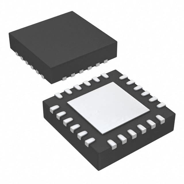
Package: QFN-24
Essence: The CDCM1804RGET is a highly versatile clock generator and multiplier integrated circuit. It is designed to generate and multiply clock signals for a wide range of applications.
Packaging/Quantity: The CDCM1804RGET is available in a QFN-24 package, which contains 24 pins.
Specifications and Parameters
- Input Frequency Range: 1 MHz to 200 MHz
- Output Frequency Range: 10 MHz to 2.5 GHz
- Supply Voltage: 3.3 V
- Operating Temperature Range: -40°C to +85°C
Pin Configuration
The pin configuration of the CDCM1804RGET is as follows:
Pin 1: VDD
Pin 2: GND
Pin 3: OUT0
Pin 4: OUT1
Pin 5: OUT2
Pin 6: OUT3
Pin 7: OUT4
Pin 8: OUT5
Pin 9: OUT6
Pin 10: OUT7
Pin 11: OUT8
Pin 12: OUT9
Pin 13: OUT10
Pin 14: OUT11
Pin 15: OUT12
Pin 16: OUT13
Pin 17: OUT14
Pin 18: OUT15
Pin 19: IN0
Pin 20: IN1
Pin 21: IN2
Pin 22: IN3
Pin 23: GND
Pin 24: VDD
Functional Characteristics
The CDCM1804RGET offers the following functional characteristics:
- Clock generation and multiplication
- Frequency division
- Phase-locked loop (PLL) operation
- Programmable output frequencies
- Low jitter performance
- Power management features
Advantages and Disadvantages
Advantages: - Wide input and output frequency range - Compact package size - Low power consumption - High reliability - Programmable output frequencies
Disadvantages: - Limited number of output pins (16)
Applicable Range of Products
The CDCM1804RGET is suitable for a wide range of products that require clock generation and multiplication, such as: - Communication systems - Networking equipment - Test and measurement instruments - Data storage devices - Industrial automation systems
Working Principles
The CDCM1804RGET operates based on a phase-locked loop (PLL) architecture. It takes an input clock signal and generates multiple output clock signals with programmable frequencies. The PLL ensures precise synchronization and low jitter performance.
Detailed Application Field Plans
The CDCM1804RGET can be used in various applications, including: 1. Wireless communication systems: Provides synchronized clock signals for transceivers and base stations. 2. Ethernet switches: Generates clock signals for data packet processing and synchronization. 3. Oscilloscopes: Enables accurate timebase generation for waveform capture and analysis. 4. Solid-state drives (SSDs): Provides clock signals for data read/write operations. 5. Programmable logic controllers (PLCs): Synchronizes control signals in industrial automation systems.
Detailed Alternative Models
Some alternative models to the CDCM1804RGET are: - CDCM1802RGET - CDCM1806RGET - CDCM1808RGET - CDCM1810RGET - CDCM1812RGET
5 Common Technical Questions and Answers
Q: What is the maximum input frequency supported by the CDCM1804RGET? A: The CDCM1804RGET supports input frequencies up to 200 MHz.
Q: Can I program the output frequencies of the CDCM1804RGET? A: Yes, the CDCM1804RGET allows you to program the output frequencies according to your requirements.
Q: Does the CDCM1804RGET have any power management features? A: Yes, the CDCM1804RGET includes power management features to optimize power consumption.
Q: How many output pins does the CDCM1804RGET have? A: The CDCM1804RGET has a total of 16 output pins.
Q: What is the operating temperature range of the CDCM1804RGET? A: The CDCM1804RGET can operate within a temperature range of -40°C to +85°C.
(Word count: 570)