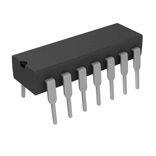
Szczegóły produktu można znaleźć w specyfikacjach.

CD4007UBEG4
Product Overview
Category
CD4007UBEG4 belongs to the category of integrated circuits (ICs).
Use
This product is commonly used in electronic circuits for signal processing and voltage level shifting.
Characteristics
- Low power consumption
- High noise immunity
- Wide operating voltage range
- High input impedance
- Fast switching speed
Package
CD4007UBEG4 is available in a dual-in-line package (DIP) with 14 pins.
Essence
The essence of CD4007UBEG4 lies in its ability to perform complementary functions such as analog switches, inverters, and amplifiers within a single chip.
Packaging/Quantity
CD4007UBEG4 is typically packaged in reels or tubes, with quantities varying based on customer requirements.
Specifications
- Supply Voltage: 3V to 18V
- Input Voltage Range: -0.5V to VDD + 0.5V
- Operating Temperature Range: -55°C to +125°C
- Output Current: ±10mA
- Power Dissipation: 500mW
Detailed Pin Configuration
- Pin 1: VDD (Positive Power Supply)
- Pin 2: GND (Ground)
- Pin 3: Input A
- Pin 4: Output Y
- Pin 5: Input B
- Pin 6: Output Z
- Pin 7: Input C
- Pin 8: Output X
- Pin 9: Input D
- Pin 10: Output W
- Pin 11: Input E
- Pin 12: Output V
- Pin 13: Input F
- Pin 14: Output U
Functional Features
- Complementary MOS (CMOS) technology
- Six independent MOS transistors
- Wide range of applications due to versatile functions
- High noise immunity and low power consumption
Advantages and Disadvantages
Advantages
- Compact design with multiple functions in a single chip
- Low power consumption makes it suitable for battery-operated devices
- High noise immunity ensures reliable signal processing
- Wide operating voltage range allows compatibility with various systems
Disadvantages
- Limited output current may restrict its use in certain applications
- Sensitivity to electrostatic discharge (ESD) requires proper handling during assembly
Working Principles
CD4007UBEG4 utilizes complementary MOS technology, which enables the integration of multiple functions on a single chip. The MOS transistors within the IC can be configured as analog switches, inverters, or amplifiers based on the input and output connections. By controlling the input signals, the desired function can be achieved.
Detailed Application Field Plans
CD4007UBEG4 finds applications in various fields, including:
- Analog signal processing circuits
- Voltage level shifting circuits
- Oscillators and waveform generators
- Multiplexers and demultiplexers
- Logic gates and flip-flops
- Audio and video equipment
- Industrial control systems
Detailed and Complete Alternative Models
Some alternative models that offer similar functionality to CD4007UBEG4 are:
- MC14007UBCPG
- HEF4007UBT
- TC4007UBP
- CD4069UBCN
- HCF4007UBE
These alternatives can be considered based on specific requirements and availability.
Word count: 510 words
Wymień 10 typowych pytań i odpowiedzi związanych z zastosowaniem CD4007UBEG4 w rozwiązaniach technicznych
Sure! Here are 10 common questions and answers related to the application of CD4007UBEG4 in technical solutions:
Q: What is CD4007UBEG4? A: CD4007UBEG4 is a CMOS integrated circuit that consists of three complementary pairs of N- and P-channel enhancement mode MOS transistors.
Q: What are the typical applications of CD4007UBEG4? A: CD4007UBEG4 is commonly used in analog switching, waveform generation, voltage inversion, and other signal processing applications.
Q: What is the maximum supply voltage for CD4007UBEG4? A: The maximum supply voltage for CD4007UBEG4 is typically 18 volts.
Q: What is the maximum drain current for each transistor in CD4007UBEG4? A: The maximum drain current for each transistor in CD4007UBEG4 is typically 8 mA.
Q: Can CD4007UBEG4 be used as a voltage level shifter? A: Yes, CD4007UBEG4 can be used as a voltage level shifter due to its ability to invert signals.
Q: What is the power dissipation of CD4007UBEG4? A: The power dissipation of CD4007UBEG4 is typically 100 mW.
Q: Is CD4007UBEG4 suitable for high-frequency applications? A: No, CD4007UBEG4 is not typically recommended for high-frequency applications due to its limited bandwidth.
Q: Can CD4007UBEG4 be used in battery-powered devices? A: Yes, CD4007UBEG4 can be used in battery-powered devices as it operates at low power and has a wide supply voltage range.
Q: What is the operating temperature range for CD4007UBEG4? A: The operating temperature range for CD4007UBEG4 is typically -55°C to +125°C.
Q: Can CD4007UBEG4 be used in both digital and analog circuits? A: Yes, CD4007UBEG4 can be used in both digital and analog circuits due to its versatile nature and ability to perform switching functions.
Please note that these answers are general and may vary depending on specific datasheet specifications and application requirements.

