

Szczegóły produktu można znaleźć w specyfikacjach.
Encyclopedia Entry: 74ALVCF162834VRG4
Product Information Overview
- Category: Integrated Circuit (IC)
- Use: Logic Level Translator
- Characteristics: High-speed, low-power consumption
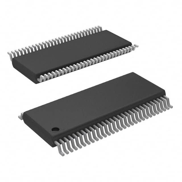
- Package: TSSOP (Thin Shrink Small Outline Package)
- Essence: Voltage level shifting between different logic families
- Packaging/Quantity: Tape and Reel, 2500 units per reel
Specifications
The 74ALVCF162834VRG4 is a logic level translator integrated circuit designed for voltage level shifting between different logic families. It operates at high speeds while consuming low power, making it suitable for various applications.
Detailed Pin Configuration
The 74ALVCF162834VRG4 has a total of 56 pins, which are arranged as follows:
- VCCB
- B0
- B1
- B2
- B3
- B4
- B5
- GND
- OE#
- A0
- A1
- A2
- A3
- A4
- A5
- VCCA
- Y0
- Y1
- Y2
- Y3
- Y4
- Y5
- GND
- Y6
- Y7
- Y8
- Y9
- Y10
- Y11
- GND
- Y12
- Y13
- Y14
- Y15
- Y16
- Y17
- GND
- Y18
- Y19
- Y20
- Y21
- Y22
- Y23
- GND
- Y24
- Y25
- Y26
- Y27
- Y28
- Y29
- GND
- Y30
- Y31
- VCCB
- B6
- B7
Functional Features
The 74ALVCF162834VRG4 offers the following functional features:
- Voltage level shifting between different logic families.
- High-speed operation, enabling efficient data transmission.
- Low power consumption, making it suitable for battery-powered devices.
- Bidirectional translation capability, allowing for seamless communication between different logic levels.
Advantages and Disadvantages
Advantages: - High-speed operation facilitates fast data transfer. - Low power consumption extends battery life in portable applications. - Bidirectional translation enables versatile usage scenarios.
Disadvantages: - Limited voltage range compatibility with specific logic families. - Requires careful consideration of input and output voltage levels to ensure proper functionality.
Working Principles
The 74ALVCF162834VRG4 operates based on voltage level shifting principles. It utilizes internal circuitry to convert input signals from one logic family to another, allowing for seamless communication between devices operating at different voltage levels. The IC ensures reliable data transmission by maintaining signal integrity and minimizing noise interference.
Detailed Application Field Plans
The 74ALVCF162834VRG4 finds applications in various fields, including but not limited to:
- Microcontroller interfacing with different logic families.
- Communication systems requiring voltage level translation.
- Industrial automation and control systems.
- Consumer electronics devices.
- Automotive electronics.
Detailed and Complete Alternative Models
Alternative models that offer similar functionality to the 74ALVCF162834VRG4 include:
- SN74LVC8T245PW - Logic Level Translator IC with 8-bit bidirectional voltage translation.
- CD4050BE - Hex Non-Inverting Buffer/Converter for voltage level shifting.
- TXB0104PWR - 4-Bit Bidirectional Voltage-Level Translator.
These alternative models provide options for different voltage ranges, package types, and pin configurations, allowing users to choose the most suitable option for their specific requirements.
Word count: 440 words
Wymień 10 typowych pytań i odpowiedzi związanych z zastosowaniem 74ALVCF162834VRG4 w rozwiązaniach technicznych
Sure! Here are 10 common questions and answers related to the application of 74ALVCF162834VRG4 in technical solutions:
Q: What is the 74ALVCF162834VRG4? A: The 74ALVCF162834VRG4 is a 16-bit universal bus driver with 3-state outputs, designed for high-speed applications.
Q: What is the maximum operating voltage for this device? A: The maximum operating voltage for the 74ALVCF162834VRG4 is typically 3.6 volts.
Q: Can I use this device in a low-power application? A: Yes, the 74ALVCF162834VRG4 is designed to operate at low power levels, making it suitable for battery-powered devices.
Q: What is the output current capability of this device? A: The 74ALVCF162834VRG4 has a typical output current capability of ±24 mA.
Q: Is this device compatible with other logic families? A: Yes, the 74ALVCF162834VRG4 is designed to be compatible with both TTL and CMOS logic families.
Q: Can I use this device in a high-speed data transmission system? A: Absolutely, the 74ALVCF162834VRG4 is specifically designed for high-speed applications, making it suitable for data transmission systems.
Q: Does this device have built-in ESD protection? A: Yes, the 74ALVCF162834VRG4 incorporates ESD protection on all inputs and outputs, ensuring robustness against electrostatic discharge.
Q: What is the typical propagation delay of this device? A: The typical propagation delay of the 74ALVCF162834VRG4 is around 2.5 ns, making it suitable for high-speed applications.
Q: Can I use this device in a bidirectional bus application? A: Yes, the 74ALVCF162834VRG4 supports bidirectional data flow, making it suitable for use in bus systems.
Q: Is this device available in different package options? A: Yes, the 74ALVCF162834VRG4 is available in various package options, such as TSSOP and TVSOP, providing flexibility in design integration.
Please note that the answers provided here are general and may vary depending on the specific datasheet and manufacturer's specifications for the 74ALVCF162834VRG4.