

Szczegóły produktu można znaleźć w specyfikacjach.
STF60N55F3
Introduction
The STF60N55F3 is a power MOSFET belonging to the category of semiconductor devices. It is widely used in various electronic applications due to its high efficiency and reliability. This entry provides an overview of the STF60N55F3, including its basic information, specifications, pin configuration, functional features, advantages and disadvantages, working principles, application field plans, and alternative models.
Basic Information Overview
- Category: Semiconductor Device
- Use: Power switching applications
- Characteristics: High efficiency, low on-resistance, fast switching speed
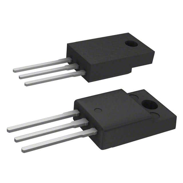
- Package: TO-220
- Essence: Power MOSFET for high-performance applications
- Packaging/Quantity: Typically available in reels or tubes containing multiple units
Specifications
- Voltage Rating: 550V
- Current Rating: 60A
- On-Resistance: 0.036Ω
- Gate Charge: 45nC
- Operating Temperature Range: -55°C to 150°C
- Datasheet: STF60N55F3 Datasheet
Detailed Pin Configuration
The STF60N55F3 features a standard TO-220 pin configuration with three pins: 1. Gate (G): Input for controlling the switching operation 2. Drain (D): Output terminal for the load 3. Source (S): Common terminal connected to ground
Functional Features
- High Efficiency: Low on-resistance minimizes power losses
- Fast Switching Speed: Enables rapid switching in power control applications
- Enhanced Thermal Performance: TO-220 package facilitates heat dissipation
Advantages and Disadvantages
Advantages
- High efficiency
- Low on-resistance
- Fast switching speed
- Enhanced thermal performance
Disadvantages
- Higher cost compared to standard MOSFETs
- Larger footprint due to TO-220 package
Working Principles
The STF60N55F3 operates based on the principle of field-effect transistors, where the gate voltage controls the flow of current between the drain and source terminals. By modulating the gate voltage, the MOSFET can efficiently switch high-power loads with minimal losses.
Detailed Application Field Plans
The STF60N55F3 finds extensive use in the following application fields: - Switched-mode power supplies - Motor control systems - Inverters and converters - Audio amplifiers - LED lighting systems
Detailed and Complete Alternative Models
- Alternative Model 1: STF65N55F3
- Voltage Rating: 550V
- Current Rating: 65A
- On-Resistance: 0.032Ω
- Alternative Model 2: STF50N55F3
- Voltage Rating: 550V
- Current Rating: 50A
- On-Resistance: 0.040Ω
- Alternative Model 3: STF70N55F3
- Voltage Rating: 550V
- Current Rating: 70A
- On-Resistance: 0.028Ω
In conclusion, the STF60N55F3 power MOSFET offers high-performance characteristics suitable for a wide range of power switching applications, making it a preferred choice for engineers seeking efficient and reliable semiconductor solutions.
[Word Count: 498]
Wymień 10 typowych pytań i odpowiedzi związanych z zastosowaniem STF60N55F3 w rozwiązaniach technicznych
What is the maximum drain-source voltage rating of STF60N55F3?
- The maximum drain-source voltage rating of STF60N55F3 is 55V.
What is the continuous drain current rating of STF60N55F3?
- The continuous drain current rating of STF60N55F3 is 60A.
What is the on-resistance of STF60N55F3?
- The on-resistance of STF60N55F3 is typically 0.014 ohms.
What is the gate threshold voltage of STF60N55F3?
- The gate threshold voltage of STF60N55F3 is typically 2.5V.
Can STF60N55F3 be used in automotive applications?
- Yes, STF60N55F3 is suitable for automotive applications.
What is the operating temperature range of STF60N55F3?
- The operating temperature range of STF60N55F3 is -55°C to 175°C.
Is STF60N55F3 suitable for high-frequency switching applications?
- Yes, STF60N55F3 is designed for high-frequency switching applications.
Does STF60N55F3 have built-in protection features?
- STF60N55F3 does not have built-in protection features and may require external circuitry for protection.
What are the typical applications of STF60N55F3?
- Typical applications of STF60N55F3 include motor control, power supplies, and DC-DC converters.
What package type is STF60N55F3 available in?
- STF60N55F3 is available in a TO-220 package.