

Szczegóły produktu można znaleźć w specyfikacjach.
NB100LVEP221FAR2
Basic Information Overview
- Category: Integrated Circuit
- Use: Signal Processing
- Characteristics: High-speed, Low-voltage Differential Signaling (LVDS) Buffer
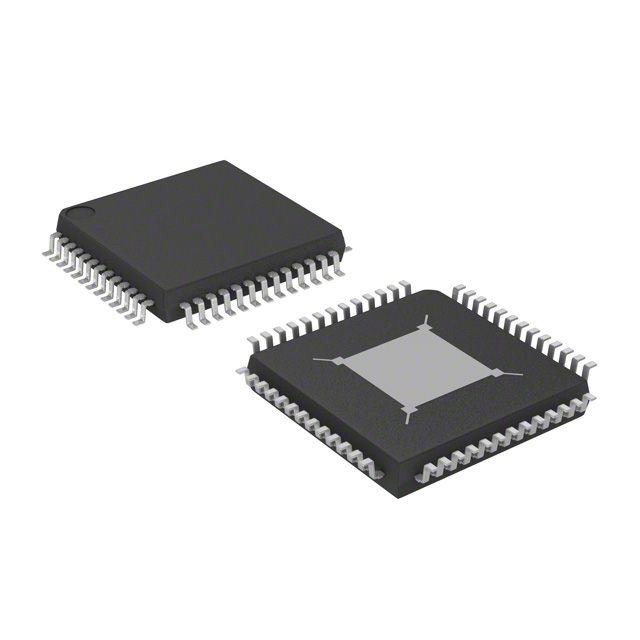
- Package: Small Outline Integrated Circuit (SOIC)
- Essence: Provides high-speed signal buffering and level shifting capabilities
- Packaging/Quantity: Tape and Reel, 2500 units per reel
Specifications and Parameters
- Supply Voltage Range: 3.0V to 3.6V
- Input Voltage Range: -0.3V to VCC + 0.3V
- Output Voltage Range: 0V to VCC
- Operating Temperature Range: -40°C to +85°C
- Maximum Input Clock Frequency: 1.5 GHz
- Output Skew: 50 ps (typical)
Detailed and Complete Pin Configuration
- VCC
- GND
- CLKIN
- CLKOUT
- LVEN
- Q0
- Q1
- Q2
- Q3
- Q4
- Q5
- Q6
- Q7
- Q8
- Q9
- Q10
- Q11
- Q12
- Q13
- Q14
- Q15
- Q16
- Q17
- Q18
- Q19
- Q20
- Q21
- Q22
- Q23
- Q24
- Q25
- Q26
- Q27
- Q28
- Q29
- Q30
- Q31
- Q32
- Q33
- Q34
- Q35
- Q36
- Q37
- Q38
- Q39
- Q40
- Q41
- Q42
- Q43
- Q44
- Q45
- Q46
- Q47
- Q48
- Q49
- Q50
- Q51
- Q52
- Q53
- Q54
- Q55
- Q56
- Q57
- Q58
- Q59
- Q60
- Q61
- Q62
- Q63
Functional Characteristics
- LVDS input and output compatibility
- High-speed clock distribution
- Low output skew
- Differential signaling for noise immunity
- Wide operating voltage range
- ESD protection on all pins
Advantages and Disadvantages
Advantages: - High-speed signal buffering - Level shifting capabilities - Low output skew - Noise immunity with differential signaling - Wide operating voltage range
Disadvantages: - Requires LVDS-compatible devices for proper operation - Limited pin configuration options
Applicable Range of Products
- Communication systems
- Data transmission equipment
- Networking devices
- Industrial automation systems
- Test and measurement instruments
Working Principles
The NB100LVEP221FAR2 is a high-speed LVDS buffer that operates by receiving an LVDS input clock signal and distributing it to multiple LVDS outputs. It provides level shifting capabilities to ensure compatibility between different voltage domains. The differential signaling used in LVDS helps minimize noise interference, making it suitable for high-speed data transmission applications.
Detailed Application Field Plans
Communication Systems: The NB100LVEP221FAR2 can be used in communication systems to distribute high-speed clock signals and ensure accurate data transmission.
Data Transmission Equipment: It can be employed in data transmission equipment to buffer and level shift clock signals, improving signal integrity and reducing data errors.
Networking Devices: The LVDS buffer can be utilized in networking devices to distribute clock signals across different components, ensuring synchronized operation.
Industrial Automation Systems: It finds application in industrial automation systems where precise timing is crucial for synchronized control of various processes.
Test and Measurement Instruments: The NB100LVEP221FAR2 can be integrated into test and measurement instruments to provide accurate clock distribution and synchronization.
Detailed Alternative Models
- NB100LVEP17
- NB100LVEP224
- NB100LVEP238
5 Common Technical Questions and Answers
Q: What is the maximum input clock frequency supported by the NB100LVEP221FAR2? A: The maximum input clock frequency is 1.5 GHz.
Q: Can the NB100LVEP221FAR2 operate with a supply voltage below 3.0V? A