

Szczegóły produktu można znaleźć w specyfikacjach.
MMBFJ309LT1G
Introduction
The MMBFJ309LT1G is a field-effect transistor (FET) belonging to the category of small signal transistors. It is commonly used in electronic circuits for amplification and switching applications due to its unique characteristics.
Basic Information Overview
- Category: Small Signal Transistor
- Use: Amplification and Switching
- Characteristics: Low power consumption, high input impedance, and fast switching speed
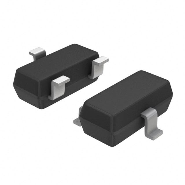
- Package: SOT-23
- Essence: N-channel JFET
- Packaging/Quantity: Available in reels of 3000 units
Specifications
- Drain-Source Voltage (VDS): 25V
- Gate-Source Voltage (VGS): ±25V
- Drain Current (ID): 50mA
- Power Dissipation (PD): 225mW
- Operating Temperature Range: -55°C to 150°C
Detailed Pin Configuration
The MMBFJ309LT1G has three pins: 1. Gate (G): Controls the conductivity between the source and drain. 2. Drain (D): Collects the current when the transistor is in the "on" state. 3. Source (S): Emits the current when the transistor is in the "on" state.
Functional Features
- High Input Impedance: Allows for minimal loading of preceding stages in an electronic circuit.
- Fast Switching Speed: Enables rapid on/off transitions, making it suitable for high-frequency applications.
- Low Power Consumption: Ideal for battery-operated devices and low-power applications.
Advantages and Disadvantages
Advantages
- Low power consumption makes it suitable for portable and battery-powered devices.
- High input impedance minimizes the impact on preceding circuitry.
- Fast switching speed enables high-frequency operation.
Disadvantages
- Limited maximum drain-source voltage compared to other FETs.
- Relatively low drain current limits its use in high-power applications.
Working Principles
The MMBFJ309LT1G operates based on the principle of field-effect modulation, where the conductivity between the source and drain is controlled by the voltage applied to the gate terminal. When a positive voltage is applied to the gate, the channel between the source and drain opens, allowing current to flow.
Detailed Application Field Plans
The MMBFJ309LT1G finds extensive use in the following applications: - Low-noise amplifiers in communication systems - Signal processing circuits in audio equipment - Switching circuits in battery-powered devices - Oscillator circuits in radio frequency (RF) applications
Detailed and Complete Alternative Models
- MMBFJ310LT1G: Similar specifications with slightly higher drain current capability.
- MMBFJ308LT1G: Lower drain-source voltage rating but similar characteristics for low-power applications.
- MMBFJ177LT1G: Higher drain current and power dissipation for more demanding applications.
In conclusion, the MMBFJ309LT1G is a versatile small signal transistor with unique characteristics that make it suitable for various amplification and switching applications, especially in low-power and high-frequency circuits.
Word Count: 456
Wymień 10 typowych pytań i odpowiedzi związanych z zastosowaniem MMBFJ309LT1G w rozwiązaniach technicznych
Sure, here are 10 common questions and answers related to the application of MMBFJ309LT1G in technical solutions:
What is MMBFJ309LT1G?
- MMBFJ309LT1G is a JFET transistor designed for high-speed switching applications.
What are the key features of MMBFJ309LT1G?
- The key features include low on-state resistance, fast switching speed, and low input capacitance.
What are the typical applications of MMBFJ309LT1G?
- Typical applications include analog switches, choppers, and high-speed switching circuits.
What is the maximum drain-source voltage for MMBFJ309LT1G?
- The maximum drain-source voltage is 25V.
What is the maximum continuous drain current for MMBFJ309LT1G?
- The maximum continuous drain current is 50mA.
What is the input capacitance of MMBFJ309LT1G?
- The input capacitance is typically 6pF.
What is the on-state resistance of MMBFJ309LT1G?
- The on-state resistance is typically 15 ohms.
Can MMBFJ309LT1G be used in high-frequency applications?
- Yes, MMBFJ309LT1G is suitable for high-frequency applications due to its fast switching speed.
Is MMBFJ309LT1G suitable for battery-powered devices?
- Yes, MMBFJ309LT1G's low on-state resistance makes it suitable for battery-powered devices where power efficiency is important.
Are there any specific layout considerations when using MMBFJ309LT1G?
- It is recommended to minimize parasitic capacitance and optimize the layout for high-speed performance when using MMBFJ309LT1G in technical solutions.