

Szczegóły produktu można znaleźć w specyfikacjach.
FJNS4202RTA Product Encyclopedia Entry
Introduction
The FJNS4202RTA is a semiconductor product belonging to the category of integrated circuits. This entry provides an overview of the basic information, specifications, pin configuration, functional features, advantages and disadvantages, working principles, application field plans, and alternative models of the FJNS4202RTA.
Basic Information Overview
- Category: Integrated Circuits
- Use: The FJNS4202RTA is commonly used in electronic devices for amplification and signal processing.
- Characteristics: It is known for its high performance, low power consumption, and compact size.
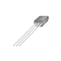
- Package: The FJNS4202RTA is typically available in small outline transistor (SOT) packages.
- Essence: The essence of this product lies in its ability to amplify and process electrical signals efficiently.
- Packaging/Quantity: It is usually packaged in reels or tubes containing multiple units.
Specifications
- Type: NPN Bipolar Junction Transistor (BJT)
- Maximum Power Dissipation: 500mW
- Collector-Base Voltage: 40V
- Collector Current: 200mA
- Transition Frequency: 250MHz
- Operating Temperature Range: -55°C to 150°C
Detailed Pin Configuration
The FJNS4202RTA has a standard three-pin configuration: 1. Emitter (E): This pin is connected to the emitter region of the transistor. 2. Base (B): The base pin controls the transistor's conductivity. 3. Collector (C): This pin is linked to the collector region of the transistor.
Functional Features
- High frequency amplification capabilities
- Low noise and distortion
- Fast switching speed
- Wide operating temperature range
Advantages and Disadvantages
Advantages
- Compact size
- Low power consumption
- High transition frequency
- Reliable performance
Disadvantages
- Limited maximum power dissipation
- Sensitive to voltage fluctuations
Working Principles
The FJNS4202RTA operates based on the principles of bipolar junction transistors, utilizing the control of current flow between its terminals to amplify and process electrical signals.
Detailed Application Field Plans
The FJNS4202RTA finds extensive use in various applications, including: - Radio frequency (RF) amplifiers - Oscillator circuits - Signal processing in communication systems - Audio amplification in consumer electronics
Detailed and Complete Alternative Models
Some alternative models to the FJNS4202RTA include: - FJNS4201RTA - FJNS4203RTA - FJNS4204RTA
In conclusion, the FJNS4202RTA is a versatile integrated circuit with high-frequency amplification capabilities, making it suitable for a wide range of electronic applications.
Word count: 398
Wymień 10 typowych pytań i odpowiedzi związanych z zastosowaniem FJNS4202RTA w rozwiązaniach technicznych
What is FJNS4202RTA?
- FJNS4202RTA is a high-performance, multi-purpose electronic component used in technical solutions for various applications.
What are the key features of FJNS4202RTA?
- The key features of FJNS4202RTA include high power handling capability, low noise figure, wide frequency range, and excellent linearity.
How is FJNS4202RTA typically used in technical solutions?
- FJNS4202RTA is commonly used in RF amplifiers, low-noise amplifiers (LNAs), and other signal processing circuits to enhance performance.
What are the recommended operating conditions for FJNS4202RTA?
- The recommended operating conditions for FJNS4202RTA include specific voltage and current requirements, as well as temperature ranges for optimal performance.
What are the potential applications of FJNS4202RTA in technical solutions?
- FJNS4202RTA can be used in applications such as wireless communication systems, radar systems, test and measurement equipment, and more.
Are there any specific design considerations when using FJNS4202RTA in technical solutions?
- Design considerations may include impedance matching, thermal management, and proper biasing to ensure the best performance of FJNS4202RTA.
What are the advantages of using FJNS4202RTA over other similar components?
- FJNS4202RTA offers superior performance in terms of noise figure, linearity, and power handling, making it a preferred choice for many technical solutions.
Are there any known limitations or challenges when using FJNS4202RTA in technical solutions?
- Some limitations may include sensitivity to improper handling, susceptibility to ESD damage, and the need for careful PCB layout and grounding.
What are the typical test and measurement procedures for evaluating FJNS4202RTA in technical solutions?
- Test and measurement procedures may involve characterizing parameters such as gain, noise figure, linearity, and power handling under various operating conditions.
Where can I find additional resources or support for integrating FJNS4202RTA into my technical solution?
- Additional resources and support can be found through the manufacturer's datasheets, application notes, and technical support channels.