

Szczegóły produktu można znaleźć w specyfikacjach.
Encyclopedia Entry: 74LVCH322244AEC/G
Product Overview
Category
The 74LVCH322244AEC/G belongs to the category of integrated circuits (ICs).
Use
This IC is commonly used for signal amplification and buffering in various electronic devices.
Characteristics
- Low-voltage operation
- High-speed performance
- Wide operating temperature range
- Low power consumption
Package
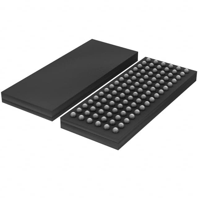
The 74LVCH322244AEC/G is available in a small outline integrated circuit (SOIC) package.
Essence
The essence of this product lies in its ability to amplify and buffer signals effectively, ensuring reliable data transmission within electronic systems.
Packaging/Quantity
The 74LVCH322244AEC/G is typically packaged in reels or tubes, with each containing a specific quantity of ICs. The exact packaging and quantity may vary depending on the supplier.
Specifications
- Supply Voltage: 1.2V - 3.6V
- Input Voltage Range: GND - VCC
- Output Voltage Range: GND - VCC
- Operating Temperature Range: -40°C to +85°C
- Number of Channels: 8
- Logic Family: LVCH
Detailed Pin Configuration
The 74LVCH322244AEC/G features a total of 20 pins, which are assigned specific functions as follows:
- Pin 1: Output Enable (OE)
- Pin 2: Channel 1 Data Input/Output (I/O)
- Pin 3: Channel 1 Data Input/Output (I/O)
- Pin 4: Channel 2 Data Input/Output (I/O)
- Pin 5: Channel 2 Data Input/Output (I/O)
- Pin 6: Ground (GND)
- Pin 7: Channel 3 Data Input/Output (I/O)
- Pin 8: Channel 3 Data Input/Output (I/O)
- Pin 9: Channel 4 Data Input/Output (I/O)
- Pin 10: Channel 4 Data Input/Output (I/O)
- Pin 11: Supply Voltage (VCC)
- Pin 12: Channel 5 Data Input/Output (I/O)
- Pin 13: Channel 5 Data Input/Output (I/O)
- Pin 14: Channel 6 Data Input/Output (I/O)
- Pin 15: Channel 6 Data Input/Output (I/O)
- Pin 16: Channel 7 Data Input/Output (I/O)
- Pin 17: Channel 7 Data Input/Output (I/O)
- Pin 18: Channel 8 Data Input/Output (I/O)
- Pin 19: Channel 8 Data Input/Output (I/O)
- Pin 20: Output Enable (OE)
Functional Features
- Signal amplification and buffering for reliable data transmission
- High-speed operation for efficient signal processing
- Low-voltage operation for reduced power consumption
- Wide operating temperature range for versatile applications
Advantages and Disadvantages
Advantages
- High-speed performance enables rapid data transfer
- Low-voltage operation reduces power consumption
- Wide operating temperature range allows usage in various environments
Disadvantages
- Limited number of channels (8) may not be sufficient for complex systems requiring more inputs/outputs
- Specific pin configuration may require careful consideration during circuit design
Working Principles
The 74LVCH322244AEC/G operates by receiving input signals through its data input pins and amplifying/buffering them before transmitting to the corresponding output pins. The output enable pins control the activation of the output channels, allowing for selective data transmission.
Detailed Application Field Plans
The 74LVCH322244AEC/G finds applications in various electronic systems, including but not limited to: - Communication devices - Computer peripherals - Industrial automation equipment - Automotive electronics - Consumer electronics
Detailed and Complete Alternative Models
- 74HC322244: Similar functionality with a different logic family (HC).
- SN74LVCH322244A: Equivalent IC from a different manufacturer.
- MC74LVCH322244: Alternative model with comparable specifications.
These alternative models offer similar signal amplification and buffering capabilities, catering to diverse design requirements.
Word Count: 450 words
Wymień 10 typowych pytań i odpowiedzi związanych z zastosowaniem 74LVCH322244AEC/G: w rozwiązaniach technicznych
What is the maximum operating voltage of 74LVCH322244AEC/G?
- The maximum operating voltage is 3.6V.What is the typical propagation delay of 74LVCH322244AEC/G?
- The typical propagation delay is 4.5ns.Can 74LVCH322244AEC/G be used for level shifting applications?
- Yes, it can be used for level shifting between different voltage domains.What is the input voltage range for 74LVCH322244AEC/G?
- The input voltage range is 0V to 5.5V.Is 74LVCH322244AEC/G suitable for buffer and line driver applications?
- Yes, it is suitable for both buffer and line driver applications.Does 74LVCH322244AEC/G have overvoltage protection?
- No, it does not have built-in overvoltage protection.Can 74LVCH322244AEC/G be used in automotive applications?
- Yes, it is AEC-Q100 qualified and suitable for automotive applications.What is the maximum output current of 74LVCH322244AEC/G?
- The maximum output current is ±24mA per channel.Is 74LVCH322244AEC/G compatible with standard CMOS levels?
- Yes, it is compatible with standard CMOS levels.What is the package type of 74LVCH322244AEC/G?
- It is available in TSSOP and TVSOP packages.