

Szczegóły produktu można znaleźć w specyfikacjach.
Encyclopedia Entry: 74LVC2G241DC-Q100H
Product Overview
- Category: Integrated Circuit (IC)
- Use: Signal Buffer/Driver
- Characteristics: Low-voltage, dual gate, non-inverting buffer/driver
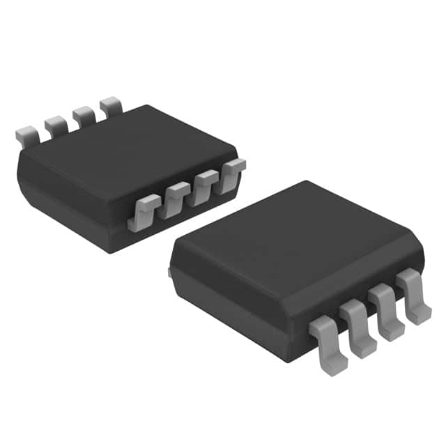
- Package: 8-pin DFN (Dual Flat No-leads) package
- Essence: Provides signal buffering and driving capabilities in low-voltage applications
- Packaging/Quantity: Available in reels of 3000 units
Specifications
- Supply Voltage Range: 1.65V to 5.5V
- Input Voltage Range: GND to VCC
- Output Voltage Range: GND to VCC
- Operating Temperature Range: -40°C to +125°C
- Propagation Delay: 4.3 ns (typical)
- Output Drive Capability: ±24 mA
- Input Capacitance: 3 pF (typical)
- Output Capacitance: 6 pF (typical)
Detailed Pin Configuration
The 74LVC2G241DC-Q100H IC has the following pin configuration:
___________
   A1 |           | VCC
   A2 |           | B1
   OE |           | B2
  GND |           | Y1
   Y2 |           | NC
       ‾‾‾‾‾‾‾‾‾‾‾‾
Functional Features
- Dual gate design allows independent control of two separate signals (A and B)
- Non-inverting buffer/driver ensures that the output signal matches the input signal
- Low-voltage operation makes it suitable for battery-powered devices
- High-speed propagation delay enables efficient signal transmission
- Output drive capability allows for driving capacitive loads
- Wide supply voltage range provides flexibility in various applications
Advantages and Disadvantages
Advantages: - Dual gate design enables versatile signal control - Non-inverting buffer/driver ensures signal integrity - Low-voltage operation makes it suitable for portable devices - High-speed propagation delay facilitates efficient signal transmission
Disadvantages: - Limited output drive capability may not be suitable for high-current applications - 8-pin package may limit the number of available I/O pins in complex designs
Working Principles
The 74LVC2G241DC-Q100H is a dual gate buffer/driver IC that operates at low voltages. It takes two input signals (A1 and A2) and provides two corresponding output signals (Y1 and Y2). The non-inverting nature of the buffer ensures that the output signals match the input signals. The IC can be enabled or disabled using the OE (Output Enable) pin.
Detailed Application Field Plans
The 74LVC2G241DC-Q100H IC finds applications in various fields, including: 1. Portable Electronics: Due to its low-voltage operation and compact package, it is suitable for use in smartphones, tablets, and wearable devices. 2. Automotive Electronics: The IC's wide operating temperature range and automotive-grade qualification make it ideal for automotive applications such as infotainment systems and engine control units. 3. Industrial Automation: Its high-speed propagation delay and output drive capability make it suitable for industrial automation systems, including motor control and sensor interfacing.
Detailed and Complete Alternative Models
Some alternative models that offer similar functionality to the 74LVC2G241DC-Q100H IC include: - SN74LVC2G241DBVR - MC74LVC2G241DTG - TC7SZU241AFK
These alternative models have comparable specifications and pin configurations, providing options for different sourcing preferences or availability.
Word count: 439 words
Wymień 10 typowych pytań i odpowiedzi związanych z zastosowaniem 74LVC2G241DC-Q100H w rozwiązaniach technicznych
Sure! Here are 10 common questions and answers related to the application of 74LVC2G241DC-Q100H in technical solutions:
Q: What is the 74LVC2G241DC-Q100H? A: The 74LVC2G241DC-Q100H is a dual buffer/line driver IC that operates at a voltage range of 1.65V to 5.5V.
Q: What is the purpose of the 74LVC2G241DC-Q100H? A: This IC is commonly used for signal buffering, level shifting, and line driving applications in various electronic circuits.
Q: What is the maximum operating frequency of the 74LVC2G241DC-Q100H? A: The maximum operating frequency of this IC is typically around 200 MHz.
Q: Can the 74LVC2G241DC-Q100H be used with both CMOS and TTL logic levels? A: Yes, this IC is compatible with both CMOS and TTL logic levels, making it versatile for different applications.
Q: What is the output drive capability of the 74LVC2G241DC-Q100H? A: The output drive capability of this IC is typically around 24 mA, allowing it to drive moderate loads.
Q: Does the 74LVC2G241DC-Q100H have built-in protection features? A: Yes, this IC has built-in protection against electrostatic discharge (ESD) and excessive power dissipation.
Q: Can the 74LVC2G241DC-Q100H be used in automotive applications? A: Yes, the "Q100" designation in the part number indicates that this IC is qualified for automotive applications.
Q: What is the package type of the 74LVC2G241DC-Q100H? A: This IC is available in a small SOT353 package, which is suitable for space-constrained designs.
Q: Can the 74LVC2G241DC-Q100H be used in battery-powered devices? A: Yes, this IC has a wide operating voltage range and low power consumption, making it suitable for battery-powered applications.
Q: Are there any application notes or reference designs available for the 74LVC2G241DC-Q100H? A: Yes, the manufacturer provides application notes and reference designs that can help users understand and implement this IC effectively.
Please note that the answers provided here are general and may vary depending on specific datasheet specifications and application requirements.