

Szczegóły produktu można znaleźć w specyfikacjach.
74HC3G06GD,125
Basic Information Overview
- Category: Integrated Circuit (IC)
- Use: Logic Gate Buffer/Inverter
- Characteristics: High-speed operation, low power consumption
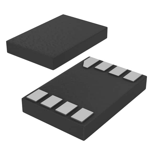
- Package: SOT753
- Essence: Triple Inverter with Open Drain Output
- Packaging/Quantity: Tape and Reel, 3000 pieces per reel
Specifications
- Supply Voltage Range: 2.0V to 6.0V
- Input Voltage Range: -0.5V to VCC + 0.5V
- Output Voltage Range: -0.5V to VCC + 0.5V
- Operating Temperature Range: -40°C to +125°C
- Propagation Delay: 4.5ns (typical) at 4.5V supply voltage
Detailed Pin Configuration
The 74HC3G06GD,125 has a total of six pins: 1. GND: Ground pin 2. A: Input pin for the first inverter 3. Y: Output pin for the first inverter 4. B: Input pin for the second inverter 5. Z: Output pin for the second inverter 6. C: Input pin for the third inverter
Functional Features
- Triple inverter with open drain output
- High-speed operation allows for quick signal processing
- Low power consumption makes it suitable for battery-powered devices
- Open drain output enables easy interfacing with other devices
- Wide supply voltage range provides flexibility in various applications
Advantages and Disadvantages
Advantages: - High-speed operation ensures efficient signal processing - Low power consumption extends battery life in portable devices - Open drain output simplifies interfacing with other components - Wide supply voltage range allows for versatile applications
Disadvantages: - Limited number of inverters (three) in a single package - May not be suitable for applications requiring a large number of logic gates
Working Principles
The 74HC3G06GD,125 is based on CMOS technology and operates as a triple inverter. It takes the input signal and produces the inverted output signal. The open drain output allows the device to either pull the output low or leave it floating, depending on the connected circuitry. This IC operates within a specified supply voltage range and provides fast propagation delay for efficient signal processing.
Detailed Application Field Plans
The 74HC3G06GD,125 can be used in various applications, including: 1. Digital communication systems 2. Microcontrollers and microprocessors 3. Industrial automation 4. Consumer electronics 5. Automotive electronics
Detailed and Complete Alternative Models
Some alternative models that can be considered are: 1. SN74LVC3G06: Triple Inverter with Open Drain Output, VCC = 1.65V to 5.5V 2. MC74VHC1G06: Single Inverter with Open Drain Output, VCC = 2.0V to 5.5V 3. CD4049UB: Hex Inverting Buffer/Converter, VCC = 3.0V to 18V
These alternative models offer similar functionality and can be used as substitutes depending on specific requirements.
In conclusion, the 74HC3G06GD,125 is a triple inverter IC with open drain output. Its high-speed operation, low power consumption, and wide supply voltage range make it suitable for various applications. However, it has a limited number of inverters in a single package. Alternative models provide additional options based on specific needs.
Wymień 10 typowych pytań i odpowiedzi związanych z zastosowaniem 74HC3G06GD,125 w rozwiązaniach technicznych
Sure! Here are 10 common questions and answers related to the application of 74HC3G06GD,125 in technical solutions:
Q: What is the function of the 74HC3G06GD,125? A: The 74HC3G06GD,125 is a triple inverter gate with open-drain outputs. It can be used for signal inversion and level shifting.
Q: What is the voltage supply range for the 74HC3G06GD,125? A: The 74HC3G06GD,125 operates with a voltage supply range of 2 V to 6 V.
Q: Can the 74HC3G06GD,125 handle high-speed signals? A: Yes, the 74HC3G06GD,125 is designed to operate at high speeds, making it suitable for applications requiring fast signal processing.
Q: How many inverters are there in the 74HC3G06GD,125? A: The 74HC3G06GD,125 consists of three independent inverters.
Q: What is the maximum output current of the 74HC3G06GD,125? A: The maximum output current per channel of the 74HC3G06GD,125 is typically 8 mA.
Q: Can the 74HC3G06GD,125 be used in both CMOS and TTL logic systems? A: Yes, the 74HC3G06GD,125 is compatible with both CMOS and TTL logic levels, allowing for versatile integration into various systems.
Q: Does the 74HC3G06GD,125 have built-in protection features? A: Yes, the 74HC3G06GD,125 has built-in protection against electrostatic discharge (ESD) and excessive power dissipation.
Q: What is the operating temperature range for the 74HC3G06GD,125? A: The 74HC3G06GD,125 can operate within a temperature range of -40°C to +125°C.
Q: Can the 74HC3G06GD,125 be used in battery-powered applications? A: Yes, the 74HC3G06GD,125 has a low power consumption, making it suitable for battery-powered devices.
Q: Are there any recommended application circuits available for the 74HC3G06GD,125? A: Yes, the datasheet of the 74HC3G06GD,125 provides several recommended application circuits that can help with its integration into different technical solutions.
Please note that the answers provided here are general and may vary depending on specific design requirements and conditions. It's always recommended to refer to the datasheet and consult with technical experts for accurate information and guidance.