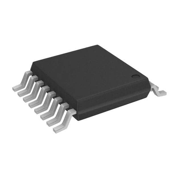
Szczegóły produktu można znaleźć w specyfikacjach.

74CB3Q3253PWJ
Basic Information Overview
- Category: Integrated Circuit (IC)
- Use: Multiplexer/Demultiplexer Switch
- Characteristics: High-speed, low-power consumption
- Package: TSSOP (Thin Shrink Small Outline Package)
- Essence: Digital logic circuit for signal routing and selection
- Packaging/Quantity: Tape and Reel, 2500 units per reel
Specifications
- Supply Voltage: 1.65V to 5.5V
- Input Voltage Range: GND to VCC
- Operating Temperature Range: -40°C to +85°C
- On-state Resistance: 4Ω (typical)
- Bandwidth: 500MHz (typical)
Detailed Pin Configuration
The 74CB3Q3253PWJ has a total of 16 pins arranged in a TSSOP package. The pin configuration is as follows:
___________
      |           |
   1  |1        16| VCC
   2  |2        15| IN0
   3  |3        14| IN1
   4  |4        13| EN
   5  |5        12| OUT1
   6  |6        11| OUT0
   7  |7        10| GND
   8  |__________|
Functional Features
- Dual 1-of-4 multiplexer/demultiplexer switch
- Low ON-state resistance for minimal signal distortion
- Wide operating voltage range for compatibility with various systems
- Fast switching speed for high-speed data transmission
- Low power consumption for energy-efficient applications
- ESD protection on all inputs and outputs for enhanced reliability
Advantages and Disadvantages
Advantages: - High-speed operation allows for efficient data routing - Low power consumption reduces energy usage and extends battery life - Wide operating voltage range ensures compatibility with different systems - ESD protection enhances the reliability of the IC
Disadvantages: - Limited number of input/output channels (4 in this case) - May require additional circuitry for complex signal routing applications
Working Principles
The 74CB3Q3253PWJ is a multiplexer/demultiplexer switch that operates based on digital logic principles. It uses control signals to select one of the four input channels and route it to the output. The enable (EN) pin determines whether the switch is active or in a high-impedance state. When enabled, the selected input is connected to the corresponding output pin, allowing the signal to pass through. When disabled, all outputs are disconnected from the inputs, resulting in isolation between channels.
Detailed Application Field Plans
The 74CB3Q3253PWJ can be used in various applications, including: 1. Data communication systems: Multiplexing multiple data streams onto a single transmission line. 2. Audio/video equipment: Switching between different audio/video sources. 3. Test and measurement instruments: Selecting different test signals for analysis. 4. Industrial automation: Routing control signals between different components. 5. Automotive electronics: Signal routing in automotive infotainment systems.
Detailed and Complete Alternative Models
- SN74CB3Q3253PWR - Similar specifications and functionality, available in a smaller package (TSSOP-16).
- MC74CB3Q3253DG - Higher bandwidth (800MHz), suitable for applications requiring faster data transmission.
- CD74CB3Q3253E - Extended temperature range (-55°C to +125°C), suitable for harsh environments.
(Note: This list is not exhaustive and other alternative models may exist.)
Word count: 399 words
Wymień 10 typowych pytań i odpowiedzi związanych z zastosowaniem 74CB3Q3253PWJ w rozwiązaniach technicznych
Sure! Here are 10 common questions and answers related to the application of 74CB3Q3253PWJ in technical solutions:
Question: What is the purpose of the 74CB3Q3253PWJ?
- Answer: The 74CB3Q3253PWJ is a multiplexer/demultiplexer IC used for signal routing and switching in electronic circuits.Question: What voltage levels does the 74CB3Q3253PWJ support?
- Answer: The 74CB3Q3253PWJ supports voltage levels from 1.65V to 5.5V, making it compatible with a wide range of digital systems.Question: How many channels does the 74CB3Q3253PWJ have?
- Answer: The 74CB3Q3253PWJ has two independent 2:1 multiplexers/demultiplexers, providing a total of four channels.Question: Can the 74CB3Q3253PWJ handle high-speed signals?
- Answer: Yes, the 74CB3Q3253PWJ is designed to handle high-speed signals with minimal propagation delay and low ON-state resistance.Question: What is the maximum data rate supported by the 74CB3Q3253PWJ?
- Answer: The 74CB3Q3253PWJ can support data rates up to 400 Mbps, making it suitable for various high-speed applications.Question: Does the 74CB3Q3253PWJ have built-in ESD protection?
- Answer: Yes, the 74CB3Q3253PWJ features built-in ESD protection, ensuring robustness against electrostatic discharge events.Question: Can I use the 74CB3Q3253PWJ in bidirectional applications?
- Answer: Yes, the 74CB3Q3253PWJ supports bidirectional signal routing, making it suitable for applications requiring both input and output signals.Question: What is the power supply voltage range for the 74CB3Q3253PWJ?
- Answer: The 74CB3Q3253PWJ operates with a power supply voltage range from 1.65V to 5.5V, allowing flexibility in different system designs.Question: Does the 74CB3Q3253PWJ have any special features for power management?
- Answer: Yes, the 74CB3Q3253PWJ includes a power-down mode that reduces power consumption when not actively switching signals.Question: Can I cascade multiple 74CB3Q3253PWJ devices together?
- Answer: Yes, you can cascade multiple 74CB3Q3253PWJ devices to expand the number of channels or create more complex signal routing configurations.
Please note that these answers are general and may vary depending on the specific application and requirements.

