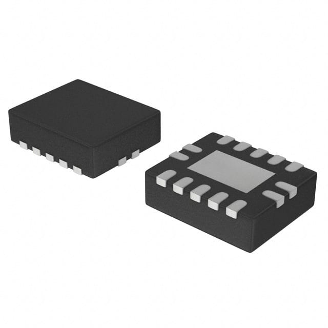
Szczegóły produktu można znaleźć w specyfikacjach.

Encyclopedia Entry: 74ALVC00BQ-Q100X
Product Overview
Category
The 74ALVC00BQ-Q100X belongs to the category of integrated circuits (ICs) and specifically falls under the family of logic gates.
Use
This product is commonly used in digital electronic systems for performing logical operations. It serves as a quad 2-input NAND gate, which means it can process two binary inputs and produce a logical NAND output.
Characteristics
- Low voltage CMOS technology
- High-speed operation
- Wide operating voltage range
- Low power consumption
- Schmitt-trigger input for noise immunity
- Compliant with automotive industry standards (AEC-Q100 Grade 1)
Package
The 74ALVC00BQ-Q100X is available in a small outline package (SOIC), which provides ease of handling and compatibility with standard PCB layouts.
Essence
The essence of this product lies in its ability to perform logical operations efficiently and reliably within digital electronic systems. It enables the implementation of complex digital circuits by providing a fundamental building block for logical functions.
Packaging/Quantity
The 74ALVC00BQ-Q100X is typically packaged in reels or tubes, containing a specific quantity of ICs per package. The exact packaging and quantity may vary depending on the manufacturer and supplier.
Specifications
- Supply Voltage Range: 1.65V to 3.6V
- Input Voltage Range: 0V to VCC
- Output Voltage Range: 0V to VCC
- Operating Temperature Range: -40°C to +125°C
- Propagation Delay: 4.5ns (typical)
- Maximum Quiescent Current: 10μA
Detailed Pin Configuration
The 74ALVC00BQ-Q100X has a total of 14 pins, each serving a specific purpose. The pin configuration is as follows:
- Input A1
- Input B1
- Output Y1
- Ground (GND)
- Input A2
- Input B2
- Output Y2
- Supply Voltage (VCC)
- Input A3
- Input B3
- Output Y3
- Input A4
- Input B4
- Output Y4
Functional Features
- Quad 2-input NAND gate functionality
- High-speed operation allows for efficient processing of logical operations
- Low power consumption ensures energy efficiency in electronic systems
- Schmitt-trigger input provides noise immunity, enhancing signal integrity
- Wide operating voltage range enables compatibility with various digital systems
- Compliance with automotive industry standards makes it suitable for automotive applications
Advantages and Disadvantages
Advantages
- High-speed operation facilitates fast data processing
- Low power consumption reduces energy requirements
- Wide operating voltage range enhances versatility
- Schmitt-trigger input improves noise immunity
- Compliance with automotive industry standards ensures reliability in automotive applications
Disadvantages
- Limited to quad 2-input NAND gate functionality
- May not be suitable for applications requiring different logic functions
Working Principles
The 74ALVC00BQ-Q100X operates based on the principles of complementary metal-oxide-semiconductor (CMOS) technology. It utilizes transistors to implement the logical NAND function, where the output is low only when both inputs are high. By controlling the voltage levels at the inputs, the IC processes logical operations and produces the corresponding output.
Detailed Application Field Plans
The 74ALVC00BQ-Q100X finds extensive use in various digital electronic systems, including but not limited to: - Microcontrollers - Data communication devices - Automotive electronics - Industrial control systems - Consumer electronics
Detailed and Complete Alternative Models
There are several alternative models available that offer similar functionality to the 74ALVC00BQ-Q100X. Some notable alternatives include: - 74HC00: High-speed CMOS quad 2-input NAND gate - 74LS00: Low-power Schottky quad 2-input NAND gate - CD4011: CMOS quad 2-input NAND gate
These alternative models provide options for different voltage ranges, power consumption levels, and package types, allowing designers to choose the most suitable option for their specific application.
Word count: 570 words
Wymień 10 typowych pytań i odpowiedzi związanych z zastosowaniem 74ALVC00BQ-Q100X w rozwiązaniach technicznych
Sure! Here are 10 common questions and answers related to the application of 74ALVC00BQ-Q100X in technical solutions:
Question: What is the function of the 74ALVC00BQ-Q100X?
Answer: The 74ALVC00BQ-Q100X is a quad 2-input NAND gate that can be used for logic operations in various electronic circuits.Question: What is the operating voltage range of the 74ALVC00BQ-Q100X?
Answer: The 74ALVC00BQ-Q100X operates within a voltage range of 1.65V to 3.6V.Question: Can the 74ALVC00BQ-Q100X be used in battery-powered devices?
Answer: Yes, the low operating voltage range makes it suitable for use in battery-powered devices.Question: What is the maximum output current of the 74ALVC00BQ-Q100X?
Answer: The maximum output current of the 74ALVC00BQ-Q100X is typically 24mA.Question: Is the 74ALVC00BQ-Q100X compatible with other logic families?
Answer: Yes, the 74ALVC00BQ-Q100X is compatible with both TTL and CMOS logic families.Question: Can the 74ALVC00BQ-Q100X be used in high-speed applications?
Answer: Yes, the 74ALVC00BQ-Q100X has a propagation delay of only a few nanoseconds, making it suitable for high-speed applications.Question: Does the 74ALVC00BQ-Q100X have built-in protection against electrostatic discharge (ESD)?
Answer: Yes, the 74ALVC00BQ-Q100X has built-in ESD protection, which helps safeguard it against damage during handling and operation.Question: Can the 74ALVC00BQ-Q100X be used in automotive applications?
Answer: Yes, the 74ALVC00BQ-Q100X is qualified for automotive applications and meets the necessary standards.Question: What is the power consumption of the 74ALVC00BQ-Q100X?
Answer: The power consumption of the 74ALVC00BQ-Q100X is typically low, making it energy-efficient.Question: Are there any specific layout considerations when using the 74ALVC00BQ-Q100X?
Answer: Yes, it is recommended to follow the manufacturer's guidelines for proper PCB layout and decoupling capacitor placement to ensure optimal performance.
Please note that these answers are general and may vary depending on the specific datasheet and application requirements.

