

Szczegóły produktu można znaleźć w specyfikacjach.
M2S050-FGG896
Product Overview
Category
The M2S050-FGG896 belongs to the category of Field-Programmable Gate Arrays (FPGAs).
Use
FPGAs are integrated circuits that can be programmed and reprogrammed to perform various digital functions. The M2S050-FGG896 is specifically designed for applications requiring high-performance and flexibility.
Characteristics
- High-performance FPGA with advanced features
- Flexible and reprogrammable design
- Suitable for a wide range of applications
- Compact size and low power consumption
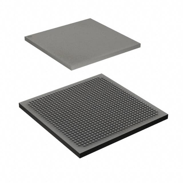
Package
The M2S050-FGG896 comes in a compact package, ensuring easy integration into electronic systems. It is designed to withstand various environmental conditions, making it suitable for both industrial and consumer applications.
Essence
The essence of the M2S050-FGG896 lies in its ability to provide a customizable and versatile solution for digital circuit implementation. Its programmable nature allows for quick prototyping and iterative development.
Packaging/Quantity
The M2S050-FGG896 is typically packaged individually and is available in various quantities depending on the requirements of the customer or project.
Specifications
- FPGA Family: M2S Series
- Model: M2S050-FGG896
- Logic Cells: 50,000
- Embedded Memory: 1,800 Kbits
- Maximum User I/Os: 396
- Operating Voltage: 1.2V
- Speed Grade: -6
- Package Type: Fine-Pitch Ball Grid Array (FGGBA)
- Package Pins: 896
- Temperature Range: -40°C to +100°C
Detailed Pin Configuration
The M2S050-FGG896 has a total of 896 pins, which are assigned to various functions such as input/output, clock signals, power supply, and configuration. The pin configuration can be found in the product datasheet provided by the manufacturer.
Functional Features
- High-performance FPGA architecture
- Configurable logic blocks for implementing complex digital circuits
- Dedicated memory blocks for efficient data storage and retrieval
- Flexible I/O interfaces for seamless integration with external devices
- Built-in clock management resources for precise timing control
- On-chip configuration memory for easy reprogramming
Advantages and Disadvantages
Advantages
- Versatile and customizable solution for digital circuit implementation
- Quick prototyping and iterative development
- High-performance capabilities for demanding applications
- Compact size and low power consumption
- Wide temperature range for diverse operating conditions
Disadvantages
- Steep learning curve for beginners due to the complexity of FPGA programming
- Higher cost compared to traditional fixed-function integrated circuits
- Limited availability of alternative models with similar specifications
Working Principles
The M2S050-FGG896 operates based on the principles of field-programmable gate arrays. It consists of configurable logic blocks, memory elements, I/O interfaces, and other supporting resources. The FPGA can be programmed using hardware description languages (HDL) or graphical tools to define the desired digital circuit functionality. Once programmed, the FPGA executes the circuit operations based on the input signals and produces the desired output.
Detailed Application Field Plans
The M2S050-FGG896 finds applications in various fields, including but not limited to: - Telecommunications - Industrial automation - Automotive electronics - Aerospace and defense - Medical devices - Consumer electronics
In telecommunications, the FPGA can be used for signal processing, protocol handling, and network optimization. In industrial automation, it enables control systems, data acquisition, and monitoring. Automotive electronics benefit from FPGAs for advanced driver assistance systems (ADAS), infotainment, and engine control. Aerospace and defense applications include radar systems, avionics, and secure communications. Medical devices utilize FPGAs for imaging, diagnostics, and patient monitoring. In consumer electronics, FPGAs are employed in gaming consoles, high-definition displays, and audio/video processing.
Detailed and Complete Alternative Models
- M2S010-FGG484
- M2S025-FGG484
- M2S040-FGG484
- M2S100-FGG484
- M2S150-FGG484
These alternative models offer similar functionality and characteristics to the M2S050-FGG896 but differ in terms of logic capacity, I/O count, and package size.
In conclusion, the M2S050-FGG896 is a high-performance FPGA that provides flexibility and versatility for various digital circuit implementations. Its compact size, low power consumption, and wide temperature range make it suitable for diverse applications across different industries. While there may be a learning curve associated with FPGA programming and a higher cost compared to fixed-function integrated circuits, the advantages of customization and performance outweigh these limitations.
Wymień 10 typowych pytań i odpowiedzi związanych z zastosowaniem M2S050-FGG896 w rozwiązaniach technicznych
Sure! Here are 10 common questions and answers related to the application of M2S050-FGG896 in technical solutions:
Q: What is M2S050-FGG896? A: M2S050-FGG896 is a specific model of field-programmable gate array (FPGA) manufactured by Microsemi.
Q: What are the key features of M2S050-FGG896? A: Some key features of M2S050-FGG896 include 50,000 logic elements, 896-ball fine-pitch BGA package, low power consumption, and high-speed performance.
Q: What are the typical applications of M2S050-FGG896? A: M2S050-FGG896 is commonly used in various technical solutions such as industrial automation, telecommunications, automotive electronics, medical devices, and aerospace systems.
Q: How can I program M2S050-FGG896? A: M2S050-FGG896 can be programmed using industry-standard hardware description languages (HDLs) like VHDL or Verilog, along with appropriate development tools provided by Microsemi.
Q: Can M2S050-FGG896 be reprogrammed after deployment? A: Yes, M2S050-FGG896 is a reprogrammable FPGA, allowing you to modify its functionality even after it has been deployed in a system.
Q: What is the power consumption of M2S050-FGG896? A: The power consumption of M2S050-FGG896 depends on the specific design and usage scenario, but it is generally known for its low power characteristics.
Q: Does M2S050-FGG896 support high-speed interfaces? A: Yes, M2S050-FGG896 supports various high-speed interfaces such as PCIe, Ethernet, USB, and DDR memory interfaces, making it suitable for applications requiring fast data transfer.
Q: Can M2S050-FGG896 interface with other components or microcontrollers? A: Yes, M2S050-FGG896 can interface with other components or microcontrollers using standard communication protocols like SPI, I2C, UART, or custom interfaces implemented in the FPGA design.
Q: What is the temperature range at which M2S050-FGG896 operates? A: M2S050-FGG896 typically operates within a temperature range of -40°C to 100°C, making it suitable for both industrial and commercial environments.
Q: Are there any development kits available for M2S050-FGG896? A: Yes, Microsemi provides development kits specifically designed for M2S050-FGG896, which include necessary hardware, software tools, and documentation to facilitate the development process.
Please note that the specific details may vary, and it's always recommended to refer to the official documentation and datasheets provided by the manufacturer for accurate information.