

Szczegóły produktu można znaleźć w specyfikacjach.
N25Q032A13ESF40G
Basic Information Overview
- Category: Non-volatile Memory
- Use: Data storage and retrieval
- Characteristics:
- High-speed performance
- Large storage capacity
- Low power consumption
- Package: SOP (Small Outline Package)
- Essence: Flash memory chip
- Packaging/Quantity: Individually packaged, quantity varies based on manufacturer
Specifications
- Capacity: 32 Megabits (4 Megabytes)
- Interface: Serial Peripheral Interface (SPI)
- Voltage Range: 2.7V to 3.6V
- Operating Temperature: -40°C to +85°C
- Erase/Program Time: Varies based on operation, typically in milliseconds
- Data Retention: Up to 20 years
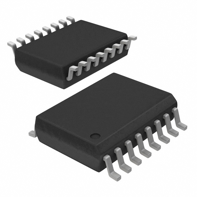
Detailed Pin Configuration
The N25Q032A13ESF40G has a total of 8 pins. The pin configuration is as follows:
- Chip Select (/CS) - Used to enable or disable the chip
- Serial Clock (SCLK) - Provides the clock signal for data transfer
- Serial Data Input (SI) - Receives data from the external device
- Serial Data Output (SO) - Transmits data to the external device
- Hold (/HOLD) - Pauses ongoing operations
- Write Protect (/WP) - Protects the memory from being written
- Ground (GND) - Reference ground
- Power Supply (VCC) - Power input for the chip
Functional Features
- High-speed Read/Write operations
- Sector erase and byte/page program functions
- Software and hardware write protection options
- Efficient power management features
- Flexible architecture for easy integration into various systems
Advantages
- Fast data access and transfer speeds
- Compact package size for space-constrained applications
- Low power consumption, suitable for battery-powered devices
- High reliability and data integrity
- Wide operating temperature range for versatile usage scenarios
Disadvantages
- Limited storage capacity compared to other memory technologies
- Relatively higher cost per unit of storage compared to traditional hard drives
- Susceptible to data loss in case of power failure during write operations
Working Principles
The N25Q032A13ESF40G is based on the NOR flash memory technology. It utilizes a grid of memory cells that store data as electrical charges. These charges are trapped within floating gate transistors, allowing the memory to retain information even when power is removed. The SPI interface enables communication between the chip and external devices, facilitating data read, write, and erase operations.
Detailed Application Field Plans
The N25Q032A13ESF40G is widely used in various electronic devices and systems, including but not limited to: - Consumer electronics (e.g., smartphones, tablets, digital cameras) - Automotive systems (e.g., infotainment systems, instrument clusters) - Industrial equipment (e.g., control systems, data loggers) - Networking devices (e.g., routers, switches) - Medical devices (e.g., patient monitors, diagnostic equipment)
Detailed and Complete Alternative Models
- N25Q032A11ESE40E
- N25Q032A13EF840E
- N25Q032A13ESE40F
- N25Q032A13ESE40G
- N25Q032A13ESE40H
These alternative models offer similar specifications and functionality, providing options for different application requirements.
Word count: 446 words
Wymień 10 typowych pytań i odpowiedzi związanych z zastosowaniem N25Q032A13ESF40G w rozwiązaniach technicznych
Sure! Here are 10 common questions and answers related to the application of N25Q032A13ESF40G in technical solutions:
Question: What is the N25Q032A13ESF40G?
Answer: The N25Q032A13ESF40G is a serial NOR flash memory chip manufactured by Micron Technology.Question: What is the storage capacity of the N25Q032A13ESF40G?
Answer: The N25Q032A13ESF40G has a storage capacity of 32 megabits (4 megabytes).Question: What is the interface used to communicate with the N25Q032A13ESF40G?
Answer: The N25Q032A13ESF40G uses the Serial Peripheral Interface (SPI) for communication.Question: What are some typical applications of the N25Q032A13ESF40G?
Answer: The N25Q032A13ESF40G is commonly used in various embedded systems, IoT devices, automotive electronics, and industrial applications that require non-volatile memory storage.Question: What is the operating voltage range of the N25Q032A13ESF40G?
Answer: The N25Q032A13ESF40G operates at a voltage range of 2.7V to 3.6V.Question: What is the maximum clock frequency supported by the N25Q032A13ESF40G?
Answer: The N25Q032A13ESF40G supports a maximum clock frequency of 104 MHz.Question: Does the N25Q032A13ESF40G support hardware and software write protection?
Answer: Yes, the N25Q032A13ESF40G supports both hardware and software write protection features to prevent accidental data modification.Question: What is the erase time for the N25Q032A13ESF40G?
Answer: The N25Q032A13ESF40G has an erase time of typically 4 seconds for a sector erase and 60 seconds for a chip erase.Question: Can the N25Q032A13ESF40G operate in extreme temperature conditions?
Answer: Yes, the N25Q032A13ESF40G is designed to operate in a wide temperature range from -40°C to +85°C.Question: Is the N25Q032A13ESF40G RoHS compliant?
Answer: Yes, the N25Q032A13ESF40G is compliant with the Restriction of Hazardous Substances (RoHS) directive.
Please note that these answers are general and may vary depending on specific product specifications and application requirements.