

Szczegóły produktu można znaleźć w specyfikacjach.
LTC6915CDE#TRPBF
Product Overview
- Category: Integrated Circuit (IC)
- Use: Amplifier
- Characteristics: High precision, low noise, wide bandwidth
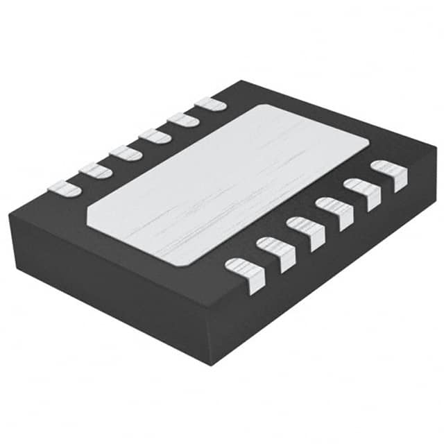
- Package: DFN-12
- Essence: Instrumentation amplifier
- Packaging/Quantity: Tape & Reel, 2500 units per reel
Specifications
- Supply Voltage Range: ±2.7V to ±5.5V
- Input Offset Voltage: ±50μV (maximum)
- Gain Bandwidth Product: 4MHz
- Input Bias Current: ±1nA (maximum)
- Operating Temperature Range: -40°C to 85°C
Detailed Pin Configuration
The LTC6915CDE#TRPBF has a total of 12 pins arranged as follows:
```
| | --| V+ V- |-- Pin 1: Positive Power Supply (V+) --| IN+ IN- |-- Pin 2: Non-Inverting Input (+IN) --| REF+ REF- |-- Pin 3: Reference Input (+REF) --| GND GND |-- Pin 4: Ground (GND) --| OUT |-- Pin 5: Output (OUT) --| NC |-- Pin 6: No Connection (NC) --| NC |-- Pin 7: No Connection (NC) --| NC |-- Pin 8: No Connection (NC) --| NC |-- Pin 9: No Connection (NC) --| NC |-- Pin 10: No Connection (NC) --| V- |-- Pin 11: Negative Power Supply (V-) |_______________|-- Pin 12: Inverting Input (-IN) ```
Functional Features
- High common-mode rejection ratio (CMRR) of 120dB
- Low input offset voltage and bias current for accurate measurements
- Wide supply voltage range allows flexibility in various applications
- Rail-to-rail output swing enables maximum dynamic range
Advantages and Disadvantages
Advantages: - High precision amplification - Low noise performance - Wide bandwidth for signal processing - Versatile supply voltage range
Disadvantages: - Limited number of pins for additional functionalities - Requires external components for specific applications
Working Principles
The LTC6915CDE#TRPBF is an instrumentation amplifier designed to amplify small differential signals accurately. It consists of three operational amplifiers configured in a differential amplifier topology. The input stage provides high common-mode rejection, while the gain stage amplifies the differential signal with high precision. The output stage ensures rail-to-rail swing for maximum signal integrity.
Detailed Application Field Plans
The LTC6915CDE#TRPBF finds applications in various fields, including:
- Precision measurement equipment: Used in data acquisition systems, medical devices, and scientific instruments to amplify low-level signals accurately.
- Industrial automation: Enables precise control and monitoring of sensors and transducers in industrial processes.
- Communication systems: Enhances signal conditioning and amplification in wireless communication devices and base stations.
- Automotive electronics: Supports sensor signal amplification in automotive applications such as engine control units and safety systems.
- Audio equipment: Provides high-fidelity amplification for audio signal processing in professional audio systems and consumer electronics.
Detailed and Complete Alternative Models
- AD8221ARZ: Instrumentation Amplifier, DIP-8 package, ±15V supply voltage range, gain bandwidth product of 1MHz.
- INA128P: Precision Instrumentation Amplifier, DIP-8 package, ±18V supply voltage range, gain bandwidth product of 200kHz.
- MCP6N11-010E/SN: Zero-Drift Instrumentation Amplifier, SOIC-8 package, ±5.5V supply voltage range, gain bandwidth product of 1MHz.
These alternative models offer similar functionality and can be considered based on specific application requirements.
Word count: 331 words
Wymień 10 typowych pytań i odpowiedzi związanych z zastosowaniem LTC6915CDE#TRPBF w rozwiązaniach technicznych
Sure! Here are 10 common questions and answers related to the application of LTC6915CDE#TRPBF in technical solutions:
Q: What is LTC6915CDE#TRPBF? A: LTC6915CDE#TRPBF is a high-speed, low-noise operational amplifier designed for various technical applications.
Q: What is the voltage supply range for LTC6915CDE#TRPBF? A: The voltage supply range for LTC6915CDE#TRPBF is typically between ±2.25V and ±6V.
Q: What is the bandwidth of LTC6915CDE#TRPBF? A: The bandwidth of LTC6915CDE#TRPBF is typically 100MHz.
Q: Can LTC6915CDE#TRPBF operate with a single power supply? A: No, LTC6915CDE#TRPBF requires a dual power supply.
Q: What is the input offset voltage of LTC6915CDE#TRPBF? A: The input offset voltage of LTC6915CDE#TRPBF is typically 0.5mV.
Q: What is the input bias current of LTC6915CDE#TRPBF? A: The input bias current of LTC6915CDE#TRPBF is typically 1nA.
Q: Can LTC6915CDE#TRPBF drive capacitive loads? A: Yes, LTC6915CDE#TRPBF can drive capacitive loads up to 100pF.
Q: What is the output voltage swing of LTC6915CDE#TRPBF? A: The output voltage swing of LTC6915CDE#TRPBF is typically ±3.9V.
Q: Is LTC6915CDE#TRPBF suitable for high-speed data acquisition applications? A: Yes, LTC6915CDE#TRPBF is well-suited for high-speed data acquisition applications due to its low noise and high bandwidth.
Q: Can LTC6915CDE#TRPBF be used in audio applications? A: Yes, LTC6915CDE#TRPBF can be used in audio applications where low noise and high bandwidth are required.
Please note that the answers provided here are general and may vary depending on specific operating conditions and requirements. It is always recommended to refer to the datasheet and consult with the manufacturer for detailed information and application-specific guidance.