

Szczegóły produktu można znaleźć w specyfikacjach.
LTC1861IS8#TRPBF
Product Overview
- Category: Integrated Circuit (IC)
- Use: Analog-to-Digital Converter (ADC)
- Characteristics: High-speed, low-power, 12-bit resolution
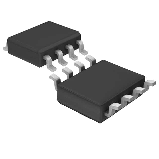
- Package: 8-pin SOIC (Small Outline Integrated Circuit)
- Essence: Converts analog signals into digital data
- Packaging/Quantity: Tape and Reel, 2500 units per reel
Specifications
- Resolution: 12 bits
- Sampling Rate: Up to 250 kSPS (thousand samples per second)
- Input Voltage Range: 0V to Vref (reference voltage)
- Power Supply: 2.7V to 5.5V
- Operating Temperature Range: -40°C to +85°C
- Conversion Time: 4.8 µs (microseconds)
- Differential Nonlinearity (DNL): ±1 LSB (Least Significant Bit)
- Integral Nonlinearity (INL): ±1 LSB
Pin Configuration
The LTC1861IS8#TRPBF has the following pin configuration:
- VIN+ (Positive Analog Input)
- VIN- (Negative Analog Input)
- VREF (Reference Voltage Input)
- GND (Ground)
- CS (Chip Select)
- SCK (Serial Clock)
- SDI (Serial Data Input)
- SDO (Serial Data Output)
Functional Features
- High-speed successive approximation ADC
- Low power consumption
- Wide input voltage range
- Internal reference voltage generator
- SPI-compatible serial interface
- Single-ended or differential input mode
- Power-down mode for reduced power consumption
Advantages and Disadvantages
Advantages: - High-speed conversion - Low power consumption - Wide input voltage range - Flexible input modes (single-ended or differential) - Easy integration with microcontrollers
Disadvantages: - Limited resolution (12 bits) - Requires an external reference voltage source - Sensitive to noise in the analog input signal
Working Principles
The LTC1861IS8#TRPBF is a high-speed, low-power ADC that converts analog signals into digital data. It utilizes a successive approximation technique to determine the digital representation of the input voltage. The analog input signal is compared to the internal reference voltage, and the conversion process iteratively approximates the input voltage by adjusting the digital output code. The converted digital data is then transmitted through the serial interface.
Detailed Application Field Plans
The LTC1861IS8#TRPBF is commonly used in various applications, including:
- Industrial Automation: Monitoring and control systems, data acquisition.
- Instrumentation: Measurement devices, sensors, signal processing.
- Communication Systems: Modems, wireless communication, base stations.
- Medical Equipment: Patient monitoring, diagnostic devices.
- Automotive Electronics: Engine control units, vehicle diagnostics.
- Consumer Electronics: Audio equipment, video processing, gaming consoles.
Detailed and Complete Alternative Models
- LTC1860IS8#TRPBF: Similar specifications, 10-bit resolution.
- LTC1862IS8#TRPBF: Higher resolution, 14-bit ADC.
- LTC1859IS8#TRPBF: Lower power consumption, 12-bit resolution.
- LTC1863IS8#TRPBF: Higher sampling rate, 12-bit resolution.
(Note: This list is not exhaustive and there may be other alternative models available.)
Word count: 440 words
Wymień 10 typowych pytań i odpowiedzi związanych z zastosowaniem LTC1861IS8#TRPBF w rozwiązaniach technicznych
Sure! Here are 10 common questions and answers related to the application of LTC1861IS8#TRPBF in technical solutions:
Q1: What is LTC1861IS8#TRPBF? A1: LTC1861IS8#TRPBF is a specific model number for a high-performance, low-power, 12-bit analog-to-digital converter (ADC) manufactured by Linear Technology.
Q2: What is the operating voltage range of LTC1861IS8#TRPBF? A2: The operating voltage range of LTC1861IS8#TRPBF is typically between 2.7V and 5.5V.
Q3: What is the maximum sampling rate of LTC1861IS8#TRPBF? A3: The maximum sampling rate of LTC1861IS8#TRPBF is 250 kilosamples per second (ksps).
Q4: What is the resolution of LTC1861IS8#TRPBF? A4: LTC1861IS8#TRPBF has a resolution of 12 bits, which means it can represent analog signals with 4096 discrete levels.
Q5: What is the input voltage range of LTC1861IS8#TRPBF? A5: The input voltage range of LTC1861IS8#TRPBF is typically between 0V and Vref, where Vref is the reference voltage provided to the ADC.
Q6: Does LTC1861IS8#TRPBF support differential inputs? A6: Yes, LTC1861IS8#TRPBF supports both single-ended and differential inputs.
Q7: What is the power consumption of LTC1861IS8#TRPBF? A7: The power consumption of LTC1861IS8#TRPBF is typically around 1.5 milliwatts (mW) during normal operation.
Q8: Can LTC1861IS8#TRPBF operate in a low-power mode? A8: Yes, LTC1861IS8#TRPBF has a power-down mode that reduces its power consumption to less than 1 micro-watt (µW).
Q9: What are the available package options for LTC1861IS8#TRPBF? A9: LTC1861IS8#TRPBF is available in an 8-pin SOIC (Small Outline Integrated Circuit) package.
Q10: What are some typical applications of LTC1861IS8#TRPBF? A10: LTC1861IS8#TRPBF is commonly used in various applications such as data acquisition systems, industrial automation, medical instrumentation, and portable devices requiring high-resolution analog-to-digital conversion.
Please note that the answers provided here are general and may vary depending on specific datasheet specifications and application requirements.