

Szczegóły produktu można znaleźć w specyfikacjach.
LTC1255CS8#PBF
Product Overview
Category
LTC1255CS8#PBF belongs to the category of integrated circuits (ICs).
Use
This product is commonly used in electronic devices for signal conditioning and amplification.
Characteristics
- LTC1255CS8#PBF is a high-performance operational amplifier.
- It operates on a single power supply voltage.
- The device offers low input offset voltage and low input bias current.
- It provides high gain bandwidth product and fast settling time.
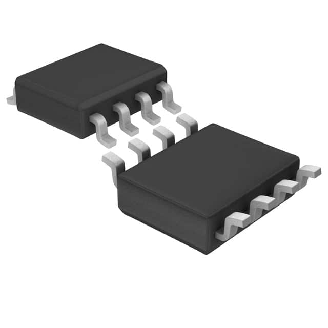
Package
LTC1255CS8#PBF comes in an 8-pin small outline package (SOIC).
Essence
The essence of LTC1255CS8#PBF lies in its ability to accurately amplify and condition signals in various electronic applications.
Packaging/Quantity
This product is typically packaged in reels or tubes, with a quantity of 250 units per reel/tube.
Specifications
- Supply Voltage: 2.7V to 36V
- Input Offset Voltage: ±1mV
- Input Bias Current: ±10nA
- Gain Bandwidth Product: 3MHz
- Settling Time: 300ns
- Operating Temperature Range: -40°C to +85°C
Detailed Pin Configuration
LTC1255CS8#PBF has the following pin configuration:
- V+ (Positive Power Supply)
- IN- (Inverting Input)
- IN+ (Non-Inverting Input)
- V- (Negative Power Supply)
- OUT (Output)
- NC (No Connection)
- NC (No Connection)
- VCC (Supply Voltage)
Functional Features
- Low input offset voltage ensures accurate signal amplification.
- High gain bandwidth product allows for precise signal conditioning.
- Fast settling time enables quick response to input changes.
- Single power supply voltage simplifies circuit design.
Advantages and Disadvantages
Advantages
- Accurate signal amplification and conditioning.
- Wide operating voltage range.
- Low input offset voltage and bias current.
- High gain bandwidth product.
- Fast settling time.
Disadvantages
- Limited number of pins for additional functionalities.
- Not suitable for applications requiring high output current.
Working Principles
LTC1255CS8#PBF operates as a voltage amplifier by amplifying the difference between its inverting and non-inverting inputs. It utilizes internal circuitry to minimize input offset voltage and bias current, ensuring accurate signal amplification. The device operates on a single power supply voltage, simplifying circuit design.
Detailed Application Field Plans
LTC1255CS8#PBF finds applications in various fields, including: 1. Audio amplifiers 2. Sensor signal conditioning 3. Data acquisition systems 4. Industrial control systems 5. Medical instrumentation
Detailed and Complete Alternative Models
Some alternative models that offer similar functionality to LTC1255CS8#PBF are: 1. AD8221 2. LM358 3. TL071 4. OP07 5. MCP6001
These models can be considered based on specific application requirements and availability.
Word count: 410 words
Wymień 10 typowych pytań i odpowiedzi związanych z zastosowaniem LTC1255CS8#PBF w rozwiązaniach technicznych
Sure! Here are 10 common questions and answers related to the application of LTC1255CS8#PBF in technical solutions:
Q: What is LTC1255CS8#PBF? A: LTC1255CS8#PBF is a specific model number for a low-power, dual, 12-bit digital-to-analog converter (DAC) manufactured by Linear Technology.
Q: What is the purpose of LTC1255CS8#PBF? A: LTC1255CS8#PBF is used to convert digital signals into analog voltages, making it suitable for various applications such as instrumentation, control systems, and audio equipment.
Q: How many channels does LTC1255CS8#PBF have? A: LTC1255CS8#PBF is a dual DAC, meaning it has two independent channels that can be used simultaneously.
Q: What is the resolution of LTC1255CS8#PBF? A: LTC1255CS8#PBF has a resolution of 12 bits, which means it can provide 4096 different output voltage levels.
Q: What is the operating voltage range of LTC1255CS8#PBF? A: LTC1255CS8#PBF operates from a single power supply voltage ranging from 2.7V to 5.5V.
Q: What is the maximum output voltage range of LTC1255CS8#PBF? A: The output voltage range of LTC1255CS8#PBF is determined by the reference voltage applied to it. It can typically swing between 0V and the reference voltage.
Q: Can LTC1255CS8#PBF handle fast switching speeds? A: Yes, LTC1255CS8#PBF is capable of fast settling times and can handle switching speeds up to several megahertz.
Q: Does LTC1255CS8#PBF have any built-in features for signal conditioning? A: Yes, LTC1255CS8#PBF includes a precision output amplifier that provides low offset voltage and low drift, enhancing the accuracy of the analog output.
Q: Can LTC1255CS8#PBF be controlled digitally? A: Yes, LTC1255CS8#PBF accepts digital input signals in various formats such as parallel, serial, or I2C, allowing for easy integration into digital control systems.
Q: Are there any application notes or reference designs available for LTC1255CS8#PBF? A: Yes, Linear Technology (now part of Analog Devices) provides extensive documentation, including application notes and reference designs, to assist engineers in implementing LTC1255CS8#PBF in their technical solutions.
Please note that the answers provided here are general and may vary depending on specific requirements and use cases. It is always recommended to refer to the manufacturer's datasheet and application notes for detailed information.