

Szczegóły produktu można znaleźć w specyfikacjach.
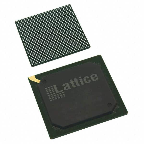
LFE3-70EA-7FN1156C
Product Overview
Category
The LFE3-70EA-7FN1156C belongs to the category of Field Programmable Gate Arrays (FPGAs).
Use
This FPGA is commonly used in electronic circuits for various applications such as digital signal processing, communication systems, and embedded systems.
Characteristics
- High-performance FPGA with advanced features
- Low power consumption
- Flexible and reconfigurable design
- High-speed data processing capabilities
Package
The LFE3-70EA-7FN1156C comes in a compact package that ensures easy integration into electronic circuit boards.
Essence
The essence of this FPGA lies in its ability to provide a customizable and programmable hardware solution for complex digital designs.
Packaging/Quantity
The LFE3-70EA-7FN1156C is typically packaged individually and is available in various quantities depending on the requirements of the user.
Specifications
- FPGA Family: LatticeECP3
- Logic Elements: 70,000
- Number of I/O Pins: 1,156
- Operating Voltage: 1.2V
- Maximum Frequency: 500 MHz
- Embedded Memory: Up to 4.8 Mb
- DSP Slices: Up to 320
- Configuration: SRAM-based
Detailed Pin Configuration
The LFE3-70EA-7FN1156C has a total of 1,156 I/O pins, which are configurable based on the specific application requirements. The pin configuration can be found in the product datasheet provided by the manufacturer.
Functional Features
- High-speed data processing capabilities
- Configurable I/O standards
- On-chip memory blocks for efficient data storage
- Built-in Digital Signal Processing (DSP) slices for complex mathematical operations
- Support for various communication protocols
- Flexible clock management resources
Advantages and Disadvantages
Advantages
- High-performance FPGA with advanced features
- Low power consumption
- Reconfigurable design allows for flexibility in system development
- Support for various communication protocols
- Efficient use of on-chip memory blocks
Disadvantages
- Limited logic elements compared to higher-end FPGAs
- Higher cost compared to simpler programmable logic devices
Working Principles
The LFE3-70EA-7FN1156C operates based on the principles of reconfigurable hardware. It consists of a matrix of configurable logic elements that can be programmed to perform specific functions. The configuration of these logic elements is stored in SRAM-based memory, allowing for easy reprogramming and customization.
Detailed Application Field Plans
The LFE3-70EA-7FN1156C finds applications in various fields, including: 1. Digital signal processing systems 2. Communication systems 3. Embedded systems 4. Industrial automation 5. Aerospace and defense
Detailed and Complete Alternative Models
- Xilinx Virtex-7 XC7VX690T FPGA
- Altera Stratix V 5SGXEA7N2F45C2 FPGA
- Microsemi SmartFusion2 M2S150 FPGA
- Intel Cyclone V GT 5CGTFD9E5F35I7N FPGA
- QuickLogic PolarPro 3 ECP3 FPGA
These alternative models offer similar capabilities and can be considered as alternatives to the LFE3-70EA-7FN1156C depending on specific requirements.
Word count: 430 words
Wymień 10 typowych pytań i odpowiedzi związanych z zastosowaniem LFE3-70EA-7FN1156C w rozwiązaniach technicznych
Sure! Here are 10 common questions and answers related to the application of LFE3-70EA-7FN1156C in technical solutions:
Q: What is the LFE3-70EA-7FN1156C? A: The LFE3-70EA-7FN1156C is a specific model of Field-Programmable Gate Array (FPGA) manufactured by Lattice Semiconductor.
Q: What are the key features of the LFE3-70EA-7FN1156C? A: The key features of this FPGA include 70,000 Look-Up Tables (LUTs), high-speed I/O interfaces, embedded memory blocks, and low power consumption.
Q: In what applications can the LFE3-70EA-7FN1156C be used? A: This FPGA can be used in various applications such as telecommunications, industrial automation, automotive electronics, medical devices, and aerospace systems.
Q: How can the LFE3-70EA-7FN1156C be programmed? A: The LFE3-70EA-7FN1156C can be programmed using Hardware Description Languages (HDLs) like VHDL or Verilog, or through graphical programming tools provided by Lattice Semiconductor.
Q: What are the advantages of using the LFE3-70EA-7FN1156C in technical solutions? A: Some advantages include its flexibility, reprogrammability, ability to handle complex logic functions, fast time-to-market, and cost-effectiveness compared to custom ASIC designs.
Q: Can the LFE3-70EA-7FN1156C interface with other components or devices? A: Yes, it can interface with various components and devices through its high-speed I/O interfaces, such as DDR memory, Ethernet controllers, ADCs, DACs, and more.
Q: What is the power consumption of the LFE3-70EA-7FN1156C? A: The power consumption of this FPGA depends on the design complexity and utilization, but it generally operates at low power levels compared to other programmable logic devices.
Q: Can the LFE3-70EA-7FN1156C be used for real-time processing applications? A: Yes, the LFE3-70EA-7FN1156C can handle real-time processing tasks due to its high-performance capabilities and fast response times.
Q: Are there any development tools or resources available for working with the LFE3-70EA-7FN1156C? A: Yes, Lattice Semiconductor provides a range of development tools, including software IDEs, simulation tools, programming cables, and documentation to aid in designing with their FPGAs.
Q: Where can I find technical support or additional information about the LFE3-70EA-7FN1156C? A: You can visit the official website of Lattice Semiconductor for technical support, datasheets, application notes, user guides, and other resources related to the LFE3-70EA-7FN1156C FPGA.