

Szczegóły produktu można znaleźć w specyfikacjach.
LFE2M70SE-7FN1152C
Product Overview
Category
The LFE2M70SE-7FN1152C belongs to the category of Field Programmable Gate Arrays (FPGAs).
Use
This FPGA is primarily used for digital logic applications, such as in embedded systems, telecommunications, and high-performance computing.
Characteristics
- High-speed processing capabilities
- Configurable logic blocks
- On-chip memory resources
- Flexible I/O interfaces
- Low power consumption
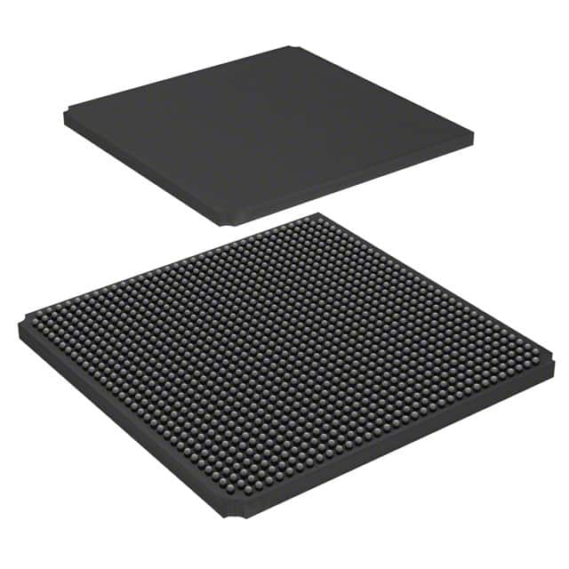
Package
The LFE2M70SE-7FN1152C comes in a compact package that ensures easy integration into electronic circuits. It is designed to be surface-mounted on printed circuit boards (PCBs).
Essence
The essence of the LFE2M70SE-7FN1152C lies in its ability to provide reconfigurable hardware that can be customized to perform specific tasks efficiently.
Packaging/Quantity
This FPGA is typically packaged in trays or reels, depending on the manufacturer's specifications. The quantity per package may vary, but it is commonly available in quantities suitable for both prototyping and production purposes.
Specifications
- Model: LFE2M70SE-7FN1152C
- Logic Elements: 70,000
- Speed Grade: 7
- Number of I/O Pins: 1,152
- Operating Voltage: 1.2V
- Package Type: FineLine BGA
- Temperature Range: -40°C to +100°C
Detailed Pin Configuration
The LFE2M70SE-7FN1152C has a comprehensive pin configuration that enables connectivity with external devices and components. The detailed pin configuration can be found in the product datasheet provided by the manufacturer.
Functional Features
- High-speed data processing
- Configurable logic blocks for flexible design implementation
- Dedicated memory resources for efficient data storage
- Versatile I/O interfaces for seamless integration with external devices
- Low power consumption for energy-efficient operation
Advantages and Disadvantages
Advantages
- High-performance capabilities
- Flexibility in design implementation
- Reconfigurable hardware for customization
- Wide range of applications
- Low power consumption
Disadvantages
- Steep learning curve for beginners
- Complex design process
- Limited availability of technical support
Working Principles
The LFE2M70SE-7FN1152C operates based on the principles of digital logic. It consists of configurable logic blocks that can be programmed to perform specific functions. These logic blocks are interconnected through programmable interconnects, allowing for the creation of complex digital circuits. The FPGA's functionality is determined by the configuration data loaded into its internal memory.
Detailed Application Field Plans
The LFE2M70SE-7FN1152C finds extensive use in various application fields, including:
- Embedded Systems: Used for implementing custom logic in microcontrollers and system-on-chip (SoC) designs.
- Telecommunications: Enables the development of high-speed communication systems, such as network routers and switches.
- High-Performance Computing: Utilized in supercomputers and data centers for parallel processing and acceleration of computational tasks.
- Industrial Automation: Facilitates the control and monitoring of industrial processes through customized logic implementations.
- Automotive Electronics: Supports advanced driver assistance systems (ADAS) and in-vehicle infotainment (IVI) systems.
Detailed and Complete Alternative Models
- LFE2M35SE-5FN672C: A smaller variant with 35,000 logic elements and 672 I/O pins.
- LFE2M100SE-6FN1152C: A larger variant with 100,000 logic elements and 1,152 I/O pins.
- LFE2M70SE-7F672C: A variant with the same logic elements but a different package type (FineLine BGA).
These alternative models provide options for different project requirements, offering varying levels of logic capacity and I/O pin count.
In conclusion, the LFE2M70SE-7FN1152C FPGA is a versatile and powerful component that enables the implementation of complex digital logic designs. Its high-speed processing capabilities, configurable logic blocks, and flexible I/O interfaces make it suitable for a wide range of applications in various industries. While it may have a steep learning curve and complex design process, its advantages outweigh the disadvantages, making it a valuable tool for digital system development.
Wymień 10 typowych pytań i odpowiedzi związanych z zastosowaniem LFE2M70SE-7FN1152C w rozwiązaniach technicznych
Sure! Here are 10 common questions and answers related to the application of LFE2M70SE-7FN1152C in technical solutions:
Q: What is LFE2M70SE-7FN1152C? A: LFE2M70SE-7FN1152C is a specific model of Field-Programmable Gate Array (FPGA) manufactured by Lattice Semiconductor.
Q: What are the key features of LFE2M70SE-7FN1152C? A: Some key features of LFE2M70SE-7FN1152C include 70,000 Look-Up Tables (LUTs), high-speed I/O interfaces, embedded memory blocks, and low power consumption.
Q: In what applications can LFE2M70SE-7FN1152C be used? A: LFE2M70SE-7FN1152C can be used in various applications such as telecommunications, industrial automation, automotive electronics, medical devices, and aerospace systems.
Q: How does LFE2M70SE-7FN1152C benefit technical solutions? A: LFE2M70SE-7FN1152C provides flexibility and reconfigurability, allowing designers to implement complex logic functions and algorithms in hardware, resulting in faster processing and improved performance.
Q: What programming languages can be used with LFE2M70SE-7FN1152C? A: LFE2M70SE-7FN1152C can be programmed using Hardware Description Languages (HDLs) such as VHDL or Verilog.
Q: Can LFE2M70SE-7FN1152C interface with other components or devices? A: Yes, LFE2M70SE-7FN1152C supports various communication protocols and interfaces like SPI, I2C, UART, Ethernet, and PCIe, enabling seamless integration with other components or devices.
Q: What is the power consumption of LFE2M70SE-7FN1152C? A: The power consumption of LFE2M70SE-7FN1152C depends on the specific design and usage scenario. However, it is designed to be power-efficient compared to traditional ASICs.
Q: Can LFE2M70SE-7FN1152C be reprogrammed after deployment? A: Yes, LFE2M70SE-7FN1152C is a reprogrammable FPGA, allowing for updates and modifications to the implemented logic even after deployment.
Q: Are there any development tools available for LFE2M70SE-7FN1152C? A: Yes, Lattice Semiconductor provides development tools like Lattice Diamond® software, which includes a complete design flow for designing, simulating, and programming LFE2M70SE-7FN1152C.
Q: Where can I find more information about LFE2M70SE-7FN1152C? A: You can find more detailed information about LFE2M70SE-7FN1152C, including datasheets, application notes, and reference designs, on the official website of Lattice Semiconductor or by contacting their technical support team.