

Szczegóły produktu można znaleźć w specyfikacjach.
LC5256MV-75FN256C
Product Overview
Category: Integrated Circuit (IC)
Use: LC5256MV-75FN256C is a programmable logic device (PLD) used for digital circuit design and implementation. It provides flexible and customizable logic functions to meet various application requirements.
Characteristics: - High-density programmable logic device - Low power consumption - Fast performance - Wide operating temperature range - RoHS compliant
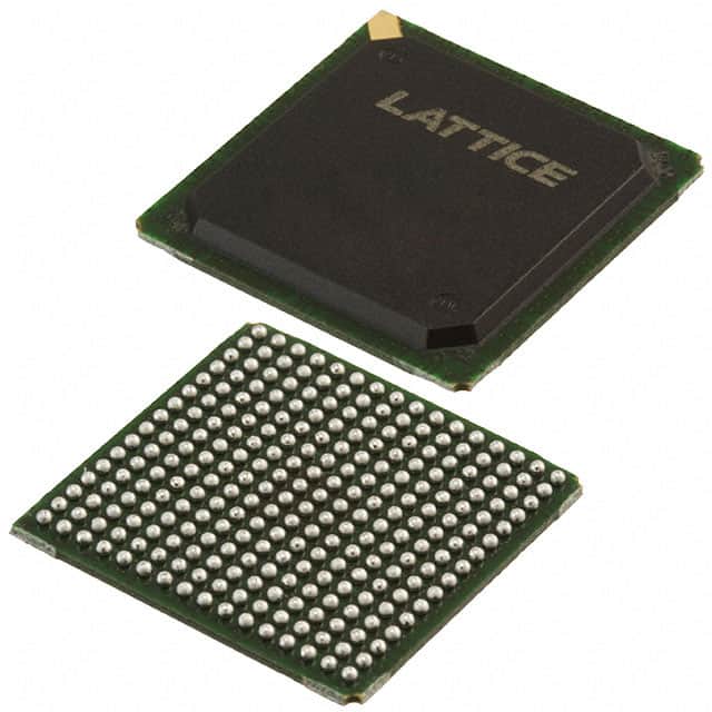
Package: LC5256MV-75FN256C is available in a 256-pin Fine-Pitch Ball Grid Array (FBGA) package, which ensures reliable electrical connections and efficient heat dissipation.
Essence: The essence of LC5256MV-75FN256C lies in its ability to provide a versatile platform for designing complex digital circuits with high efficiency and reliability.
Packaging/Quantity: LC5256MV-75FN256C is typically sold in reels or trays, with a quantity of 250 units per reel/tray.
Specifications
- Logic Cells: 5,256
- Macrocells: 75
- Operating Voltage: 3.3V
- Maximum Frequency: 100 MHz
- I/O Pins: 256
- Programmable Interconnects: 10,000
- On-Chip Memory: 64 Kbits
- Package Dimensions: 17mm x 17mm
Detailed Pin Configuration
The LC5256MV-75FN256C has a total of 256 pins, each serving a specific purpose in the circuit design. The pin configuration includes input/output pins, power supply pins, ground pins, and configuration pins. A detailed pinout diagram can be found in the product datasheet.
Functional Features
- Programmability: LC5256MV-75FN256C offers extensive programmability, allowing designers to implement custom logic functions and create complex digital circuits.
- Flexible I/O Configuration: The device provides 256 I/O pins, which can be configured as inputs or outputs based on the application requirements.
- High-Speed Performance: With a maximum operating frequency of 100 MHz, LC5256MV-75FN256C ensures fast and efficient execution of digital logic operations.
- On-Chip Memory: The integrated 64 Kbits of memory allows for storing configuration data and implementing sequential logic functions.
- Low Power Consumption: LC5256MV-75FN256C is designed to minimize power consumption, making it suitable for battery-powered applications.
Advantages and Disadvantages
Advantages: - High-density programmable logic device - Flexible and customizable logic functions - Fast performance - Wide operating temperature range - RoHS compliant
Disadvantages: - Limited macrocell count compared to higher-end PLDs - Relatively small on-chip memory capacity
Working Principles
LC5256MV-75FN256C operates based on the principles of programmable logic. It consists of an array of configurable logic cells interconnected through programmable interconnects. These logic cells can be programmed to perform various logic functions, such as AND, OR, XOR, etc. The device's behavior is determined by the configuration data stored in its on-chip memory.
Detailed Application Field Plans
LC5256MV-75FN256C finds applications in various fields, including: 1. Embedded Systems: Used for designing control systems in embedded devices like industrial automation, robotics, and automotive electronics. 2. Communications: Employed in network routers, switches, and telecommunications equipment for signal processing and protocol implementation. 3. Consumer Electronics: Utilized in smart home devices, gaming consoles, and multimedia systems for custom logic implementation. 4. Medical Devices: Integrated into medical equipment for data processing, control, and monitoring functions. 5. Aerospace and Defense: Used in avionics systems, radar systems, and military-grade electronics for high-reliability digital circuit design.
Detailed and Complete Alternative Models
- Altera MAX V CPLD Series
- Xilinx CoolRunner-II CPLD Series
- Lattice MachXO2 FPGA Series
- Microchip ATF150x CPLD Series
- Intel (formerly Altera) Cyclone IV FPGA Series
These alternative models offer similar programmable logic capabilities and can be considered as alternatives to LC5256MV-75FN256C based on specific application requirements.
Word count: 550 words
Wymień 10 typowych pytań i odpowiedzi związanych z zastosowaniem LC5256MV-75FN256C w rozwiązaniach technicznych
Sure! Here are 10 common questions and answers related to the application of LC5256MV-75FN256C in technical solutions:
Q: What is LC5256MV-75FN256C? A: LC5256MV-75FN256C is a specific model of Field Programmable Gate Array (FPGA) manufactured by Lattice Semiconductor.
Q: What are the key features of LC5256MV-75FN256C? A: Some key features of LC5256MV-75FN256C include 256 pins, 75MHz maximum operating frequency, and 5,256 logic cells.
Q: In what applications can LC5256MV-75FN256C be used? A: LC5256MV-75FN256C can be used in various applications such as industrial automation, telecommunications, automotive electronics, and consumer electronics.
Q: How can LC5256MV-75FN256C be programmed? A: LC5256MV-75FN256C can be programmed using Hardware Description Languages (HDLs) like VHDL or Verilog, or through graphical programming tools provided by Lattice Semiconductor.
Q: What is the power supply requirement for LC5256MV-75FN256C? A: LC5256MV-75FN256C typically requires a power supply voltage of 3.3V.
Q: Can LC5256MV-75FN256C interface with other components or devices? A: Yes, LC5256MV-75FN256C supports various communication protocols and interfaces like SPI, I2C, UART, and GPIOs, allowing it to interface with other components or devices.
Q: Is LC5256MV-75FN256C suitable for high-speed applications? A: Yes, LC5256MV-75FN256C can handle high-speed applications with its maximum operating frequency of 75MHz.
Q: Can LC5256MV-75FN256C be reprogrammed after initial programming? A: Yes, LC5256MV-75FN256C is a reprogrammable FPGA, allowing for multiple programming cycles during development or in the field.
Q: Are there any development tools available for working with LC5256MV-75FN256C? A: Yes, Lattice Semiconductor provides development tools like Lattice Diamond and Lattice Radiant, which offer design, simulation, and programming capabilities for LC5256MV-75FN256C.
Q: Where can I find more information about LC5256MV-75FN256C? A: You can find more detailed information about LC5256MV-75FN256C on the official website of Lattice Semiconductor or by referring to the datasheet and application notes provided by the manufacturer.