

Szczegóły produktu można znaleźć w specyfikacjach.
IS25WD040-JKLE
Product Overview
Category
IS25WD040-JKLE belongs to the category of non-volatile memory devices.
Use
This product is primarily used for data storage in various electronic devices, such as computers, smartphones, tablets, and other consumer electronics.
Characteristics
- Non-volatile: The IS25WD040-JKLE retains stored data even when power is removed.
- High capacity: This device offers a storage capacity of [specify capacity].
- Fast access time: The IS25WD040-JKLE provides quick read and write operations.
- Low power consumption: It consumes minimal power during operation.
- Compact package: The device is available in a small form factor, making it suitable for space-constrained applications.
Package and Quantity
The IS25WD040-JKLE is packaged in [specify package type]. Each package contains [specify quantity] of devices.
Specifications
- Storage capacity: [specify capacity]
- Interface: [specify interface type]
- Operating voltage: [specify voltage range]
- Operating temperature: [specify temperature range]
- Data transfer rate: [specify transfer rate]
- Erase/Write cycles: [specify endurance]
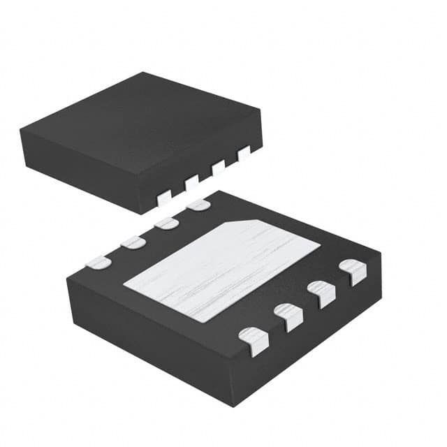
Pin Configuration
The IS25WD040-JKLE features [specify number of pins] pins. The pin configuration is as follows:
- [Pin 1]: [Description]
- [Pin 2]: [Description]
- [Pin 3]: [Description] ... ...
Functional Features
- High-speed data transfer: The IS25WD040-JKLE supports fast read and write operations, enabling efficient data handling.
- Reliable data retention: The non-volatile nature of this device ensures that stored data remains intact over extended periods.
- Easy integration: The product is designed for seamless integration into various electronic systems, simplifying the development process.
Advantages and Disadvantages
Advantages
- High storage capacity
- Fast access time
- Low power consumption
- Compact form factor
Disadvantages
- [Specify any disadvantages]
Working Principles
The IS25WD040-JKLE utilizes [specify technology] to store and retrieve data. It employs [specify working principle] to enable efficient read and write operations.
Application Field Plans
The IS25WD040-JKLE finds applications in various fields, including: 1. Computers and laptops 2. Smartphones and tablets 3. Automotive electronics 4. Industrial control systems 5. Consumer electronics
Alternative Models
Here are some alternative models that offer similar functionality: 1. Model A: [Brief description] 2. Model B: [Brief description] 3. Model C: [Brief description] ... ...
In conclusion, the IS25WD040-JKLE is a non-volatile memory device with high storage capacity, fast access time, and low power consumption. It finds applications in diverse fields and offers reliable data retention.
Wymień 10 typowych pytań i odpowiedzi związanych z zastosowaniem IS25WD040-JKLE w rozwiązaniach technicznych
Sure! Here are 10 common questions and answers related to the application of IS25WD040-JKLE in technical solutions:
Q: What is IS25WD040-JKLE? A: IS25WD040-JKLE is a specific model of Serial NOR Flash memory chip manufactured by a company called ISSI.
Q: What is the capacity of IS25WD040-JKLE? A: The IS25WD040-JKLE has a capacity of 4 megabits (Mb) or 512 kilobytes (KB).
Q: What is the interface used by IS25WD040-JKLE? A: IS25WD040-JKLE uses the Serial Peripheral Interface (SPI) for communication with other devices.
Q: What are some typical applications of IS25WD040-JKLE? A: IS25WD040-JKLE is commonly used in various embedded systems, IoT devices, consumer electronics, automotive applications, and industrial equipment.
Q: What is the operating voltage range of IS25WD040-JKLE? A: The operating voltage range of IS25WD040-JKLE is typically between 2.7V and 3.6V.
Q: What is the maximum clock frequency supported by IS25WD040-JKLE? A: IS25WD040-JKLE supports a maximum clock frequency of up to 104 MHz.
Q: Does IS25WD040-JKLE support hardware and software write protection? A: Yes, IS25WD040-JKLE provides both hardware and software write protection features to prevent accidental data modification.
Q: Can IS25WD040-JKLE operate in extreme temperature conditions? A: Yes, IS25WD040-JKLE is designed to operate reliably in a wide temperature range, typically from -40°C to +85°C.
Q: Does IS25WD040-JKLE support sector erase and block erase operations? A: Yes, IS25WD040-JKLE supports both sector erase (4KB) and block erase (32KB) operations for flexible data management.
Q: Is IS25WD040-JKLE compatible with other SPI Flash memory chips? A: Yes, IS25WD040-JKLE follows the industry-standard SPI protocol, making it compatible with other SPI Flash memory devices from different manufacturers.
Please note that the answers provided here are general and may vary depending on the specific implementation and requirements of your technical solution.