

Szczegóły produktu można znaleźć w specyfikacjach.
IS25WD020-JKLE
Product Overview
Category
IS25WD020-JKLE belongs to the category of non-volatile memory devices.
Use
This product is primarily used for data storage in various electronic devices such as computers, smartphones, tablets, and other digital devices.
Characteristics
- Non-volatile: The IS25WD020-JKLE retains stored data even when power is turned off.
- High capacity: This device offers a storage capacity of XX megabytes.
- Fast access speed: The IS25WD020-JKLE provides quick read and write operations.
- Reliable: It has a high level of data integrity and endurance.
- Compact package: The device comes in a small form factor, making it suitable for space-constrained applications.
Package and Quantity
The IS25WD020-JKLE is available in a surface-mount package. Each package contains one unit of the device.
Specifications
- Storage Capacity: XX megabytes
- Interface: SPI (Serial Peripheral Interface)
- Operating Voltage: X volts
- Operating Temperature Range: -XX°C to XX°C
- Data Retention: Up to XX years
- Erase/Program Cycles: XX,XXX cycles
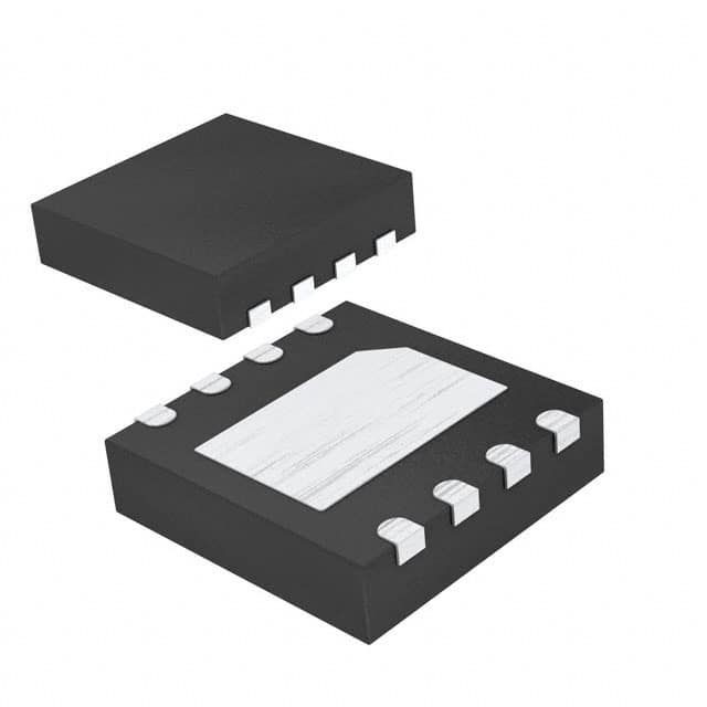
Detailed Pin Configuration
The IS25WD020-JKLE features the following pin configuration:
- VCC: Power supply voltage
- GND: Ground
- CS: Chip select
- SCK: Serial clock input
- SI: Serial data input
- SO: Serial data output
- WP: Write protect
- HOLD: Hold input
Functional Features
- High-speed data transfer: The IS25WD020-JKLE supports fast data transfer rates, enabling efficient read and write operations.
- Flexible erase and program operations: This device allows for individual sector erasure and programming, providing flexibility in managing data.
- Write protection: The WP pin can be used to protect the stored data from accidental modification.
- Hold function: The HOLD pin allows the device to pause ongoing operations without losing data.
Advantages and Disadvantages
Advantages
- High storage capacity
- Fast access speed
- Reliable data integrity
- Compact form factor
Disadvantages
- Limited erase/program cycles
- Requires an external SPI interface for communication
Working Principles
The IS25WD020-JKLE utilizes flash memory technology to store and retrieve data. It employs a Serial Peripheral Interface (SPI) for communication with the host device. The device uses a combination of floating gate transistors to store binary data in non-volatile memory cells. The data can be read, written, and erased using specific commands sent through the SPI interface.
Detailed Application Field Plans
The IS25WD020-JKLE finds applications in various electronic devices, including but not limited to: - Computers and laptops - Smartphones and tablets - Digital cameras - Gaming consoles - Industrial control systems
Alternative Models
- IS25LD020-JKLE: Similar to IS25WD020-JKLE but with additional features.
- IS25WD040-JKLE: Higher capacity version of IS25WD020-JKLE.
- IS25LD040-JKLE: Similar to IS25WD040-JKLE but with additional features.
These alternative models offer similar functionality and compatibility with different system requirements.
In conclusion, the IS25WD020-JKLE is a non-volatile memory device that provides high-speed data transfer, reliable data storage, and a compact form factor. It is widely used in various electronic devices for efficient data storage and retrieval.
Wymień 10 typowych pytań i odpowiedzi związanych z zastosowaniem IS25WD020-JKLE w rozwiązaniach technicznych
Sure! Here are 10 common questions and answers related to the application of IS25WD020-JKLE in technical solutions:
Q: What is IS25WD020-JKLE? A: IS25WD020-JKLE is a specific model of Serial NOR Flash memory chip manufactured by a company called ISSI.
Q: What is the capacity of IS25WD020-JKLE? A: The IS25WD020-JKLE has a capacity of 2 megabits (Mb), which is equivalent to 256 kilobytes (KB).
Q: What is the interface used by IS25WD020-JKLE? A: IS25WD020-JKLE uses a standard Serial Peripheral Interface (SPI) for communication with other devices.
Q: What are some typical applications of IS25WD020-JKLE? A: IS25WD020-JKLE is commonly used in various embedded systems, IoT devices, automotive electronics, industrial control systems, and consumer electronics.
Q: What is the operating voltage range of IS25WD020-JKLE? A: The operating voltage range of IS25WD020-JKLE is typically between 2.7V and 3.6V.
Q: What is the maximum data transfer rate supported by IS25WD020-JKLE? A: IS25WD020-JKLE supports a maximum data transfer rate of up to 104 MHz.
Q: Does IS25WD020-JKLE support hardware or software write protection? A: Yes, IS25WD020-JKLE supports both hardware and software write protection features to prevent accidental modification of data.
Q: Can IS25WD020-JKLE operate in extreme temperature conditions? A: Yes, IS25WD020-JKLE is designed to operate reliably in a wide temperature range, typically from -40°C to +85°C.
Q: Does IS25WD020-JKLE have any built-in error correction mechanisms? A: No, IS25WD020-JKLE does not have built-in error correction mechanisms. It relies on external error correction techniques if required.
Q: Is IS25WD020-JKLE compatible with other SPI Flash memory chips? A: Yes, IS25WD020-JKLE follows the standard SPI protocol, making it compatible with other SPI Flash memory chips from different manufacturers.
Please note that the answers provided here are general and may vary depending on the specific implementation and requirements of your technical solution.