

Szczegóły produktu można znaleźć w specyfikacjach.
EP20K600CF672C7
Basic Information Overview
- Category: Programmable Logic Device (PLD)
- Use: EP20K600CF672C7 is a PLD used for digital logic design and implementation.
- Characteristics:
- High-density programmable logic device
- Advanced architecture for complex designs
- Low power consumption
- Fast performance
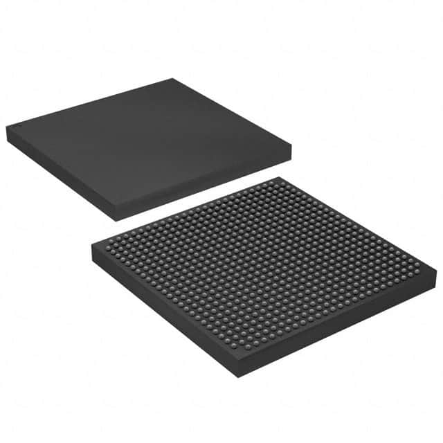
- Package: The EP20K600CF672C7 comes in a ceramic package.
- Essence: EP20K600CF672C7 is an essential component for designing and implementing digital logic circuits.
- Packaging/Quantity: The EP20K600CF672C7 is typically packaged individually and sold as a single unit.
Specifications
- Maximum Number of Logic Elements: 600,000
- Maximum Number of User I/Os: 672
- Operating Voltage: 3.3V
- Speed Grade: C7
- Package Type: Ceramic
- Temperature Range: -40°C to +85°C
Detailed Pin Configuration
The EP20K600CF672C7 has a total of 672 pins. The pin configuration is as follows:
(Pin Number) (Pin Name) 1. VCCIO 2. GND 3. TCK 4. TDI 5. TDO 6. TMS 7. JTAGEN 8. GND 9. VCCINT 10. GND 11. IO0 12. IO1 ... (remaining pins)
Functional Features
- High-density programmable logic device suitable for complex designs
- Supports various input/output standards
- Flexible and reprogrammable
- Offers advanced features like clock management and memory integration
- Provides efficient utilization of resources
Advantages
- High-performance capabilities
- Low power consumption
- Versatile and flexible for various applications
- Supports complex designs
- Offers advanced features for efficient design implementation
Disadvantages
- Relatively high cost compared to simpler logic devices
- Steeper learning curve for beginners due to complexity
Working Principles
The EP20K600CF672C7 is based on programmable logic technology. It consists of a large number of configurable logic blocks interconnected through programmable interconnects. The device can be programmed using hardware description languages (HDL) or schematic entry tools. Once programmed, the device functions as per the specified logic design.
Detailed Application Field Plans
The EP20K600CF672C7 finds application in various fields, including: 1. Telecommunications: Used in network switches, routers, and communication equipment. 2. Industrial Automation: Employed in control systems, PLCs, and robotics. 3. Aerospace and Defense: Utilized in avionics, radar systems, and military equipment. 4. Consumer Electronics: Integrated into gaming consoles, set-top boxes, and multimedia devices. 5. Automotive: Used in automotive electronics, engine control units, and infotainment systems.
Detailed and Complete Alternative Models
- EP20K400CB652C7: Similar PLD with 400,000 logic elements and 652 user I/Os.
- EP20K200FC484C7: PLD with 200,000 logic elements and 484 user I/Os.
- EP20K1000EBC652-2X: High-density PLD with 1,000,000 logic elements and 652 user I/Os.
- EP20K600EBI652-2: Enhanced version with 600,000 logic elements and 652 user I/Os.
These alternative models offer similar functionality and can be considered based on specific project requirements.
Word Count: 443 words
Wymień 10 typowych pytań i odpowiedzi związanych z zastosowaniem EP20K600CF672C7 w rozwiązaniach technicznych
Sure! Here are 10 common questions and answers related to the application of EP20K600CF672C7 in technical solutions:
Q: What is EP20K600CF672C7? A: EP20K600CF672C7 is a specific model of Field-Programmable Gate Array (FPGA) manufactured by Altera.
Q: What are the key features of EP20K600CF672C7? A: Some key features of EP20K600CF672C7 include 600,000 system gates, 672 pins, and support for various I/O standards.
Q: What are the typical applications of EP20K600CF672C7? A: EP20K600CF672C7 is commonly used in applications such as telecommunications, industrial automation, image processing, and high-performance computing.
Q: How can EP20K600CF672C7 be programmed? A: EP20K600CF672C7 can be programmed using Hardware Description Languages (HDLs) like VHDL or Verilog, or through graphical programming tools like Quartus Prime.
Q: Can EP20K600CF672C7 be reprogrammed after deployment? A: Yes, EP20K600CF672C7 is a reprogrammable FPGA, allowing for flexibility and updates even after deployment.
Q: What is the power consumption of EP20K600CF672C7? A: The power consumption of EP20K600CF672C7 depends on the specific design and usage, but it typically ranges from a few watts to tens of watts.
Q: Does EP20K600CF672C7 support external memory interfaces? A: Yes, EP20K600CF672C7 supports various external memory interfaces like DDR, SDRAM, and Flash memory.
Q: Can EP20K600CF672C7 interface with other devices or microcontrollers? A: Yes, EP20K600CF672C7 can interface with other devices or microcontrollers through various communication protocols like SPI, I2C, UART, or Ethernet.
Q: Are there any development boards available for EP20K600CF672C7? A: Yes, Altera provides development boards specifically designed for EP20K600CF672C7, which can aid in prototyping and testing.
Q: Where can I find technical documentation and support for EP20K600CF672C7? A: Technical documentation, datasheets, application notes, and support for EP20K600CF672C7 can be found on the official Altera/Intel website or community forums.