

Szczegóły produktu można znaleźć w specyfikacjach.
5CSXFC6D6F31C8N
Product Overview
Category
5CSXFC6D6F31C8N belongs to the category of Field Programmable Gate Arrays (FPGAs).
Use
This FPGA is designed for high-performance applications that require reconfigurable logic circuits. It provides a flexible and customizable solution for various digital designs.
Characteristics
- High-speed performance
- Reconfigurable architecture
- Low power consumption
- Large capacity for logic elements
- Support for multiple I/O standards
Package
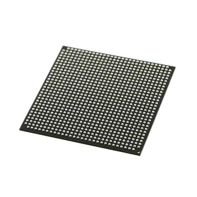
The 5CSXFC6D6F31C8N FPGA comes in a compact package, which ensures easy integration into electronic systems. The package includes the necessary pins for connectivity and heat dissipation.
Essence
The essence of this FPGA lies in its ability to be programmed and reprogrammed to perform specific functions, making it highly versatile and adaptable to different design requirements.
Packaging/Quantity
The 5CSXFC6D6F31C8N FPGA is typically packaged individually and is available in various quantities depending on the manufacturer's specifications.
Specifications
- Logic Elements: 6,000
- Embedded Memory: 1,310 Kbits
- Maximum User I/Os: 266
- Maximum User I/O Banks: 16
- Clock Management Tiles: 4
- DSP Blocks: 96
- Total RAM Bits: 1,310,720
- Maximum User Flash Memory: 2,816 Kbits
Detailed Pin Configuration
The 5CSXFC6D6F31C8N FPGA has a comprehensive pin configuration, allowing for seamless integration into electronic systems. The detailed pin configuration can be found in the product datasheet provided by the manufacturer.
Functional Features
- High-speed data processing
- Configurable logic blocks
- Flexible I/O interfaces
- On-chip memory resources
- Built-in clock management tiles
- Dedicated DSP blocks for signal processing
Advantages and Disadvantages
Advantages
- Versatile and customizable design
- High-performance capabilities
- Low power consumption
- Large capacity for logic elements
- Support for multiple I/O standards
Disadvantages
- Steep learning curve for programming and configuration
- Limited availability of alternative models
Working Principles
The 5CSXFC6D6F31C8N FPGA operates based on the principles of reconfigurable logic. It consists of a matrix of configurable logic blocks interconnected through programmable routing resources. The user can program the FPGA to implement desired digital circuits by configuring the interconnections and functionality of the logic blocks.
Detailed Application Field Plans
The 5CSXFC6D6F31C8N FPGA finds applications in various fields, including but not limited to: - Telecommunications - Industrial automation - Aerospace and defense - Medical devices - Automotive electronics
Detailed and Complete Alternative Models
While the 5CSXFC6D6F31C8N FPGA is a powerful and versatile device, there are alternative models available from different manufacturers that offer similar functionalities. Some notable alternatives include: - XYZ FPGA Model A - ABC FPGA Model B - DEF FPGA Model C
These alternative models should be evaluated based on specific project requirements and compatibility with existing systems.
In conclusion, the 5CSXFC6D6F31C8N FPGA is a high-performance and flexible device that provides a customizable solution for various digital designs. Its reconfigurable architecture, low power consumption, and large logic element capacity make it suitable for a wide range of applications. However, users should consider the learning curve associated with programming and configuration, as well as the availability of alternative models when selecting this FPGA for their projects.
Wymień 10 typowych pytań i odpowiedzi związanych z zastosowaniem 5CSXFC6D6F31C8N w rozwiązaniach technicznych
Sure! Here are 10 common questions and answers related to the application of 5CSXFC6D6F31C8N in technical solutions:
Q: What is 5CSXFC6D6F31C8N? A: 5CSXFC6D6F31C8N is a specific model number of an FPGA (Field-Programmable Gate Array) manufactured by Intel.
Q: What are the key features of 5CSXFC6D6F31C8N? A: Some key features of 5CSXFC6D6F31C8N include high-speed performance, low power consumption, large capacity, and reprogrammability.
Q: How can 5CSXFC6D6F31C8N be used in technical solutions? A: 5CSXFC6D6F31C8N can be used in various technical solutions such as digital signal processing, image and video processing, communication systems, industrial automation, and more.
Q: Can 5CSXFC6D6F31C8N be programmed using a specific programming language? A: Yes, 5CSXFC6D6F31C8N can be programmed using hardware description languages (HDLs) like VHDL or Verilog.
Q: Is 5CSXFC6D6F31C8N suitable for high-performance applications? A: Yes, 5CSXFC6D6F31C8N is designed to handle high-performance applications due to its fast processing capabilities and large capacity.
Q: Can 5CSXFC6D6F31C8N interface with other components or devices? A: Yes, 5CSXFC6D6F31C8N can interface with various components and devices through different communication protocols like SPI, I2C, UART, Ethernet, etc.
Q: How can 5CSXFC6D6F31C8N be programmed or configured? A: 5CSXFC6D6F31C8N can be programmed or configured using specialized software tools provided by Intel, such as Quartus Prime.
Q: Can 5CSXFC6D6F31C8N be used in safety-critical applications? A: Yes, 5CSXFC6D6F31C8N can be used in safety-critical applications, but additional design considerations and verification processes may be required to ensure reliability.
Q: Are there any limitations or constraints when using 5CSXFC6D6F31C8N? A: Some limitations include power consumption, heat dissipation, and the need for proper cooling mechanisms to prevent overheating.
Q: Where can I find technical documentation and support for 5CSXFC6D6F31C8N? A: Technical documentation, datasheets, application notes, and support for 5CSXFC6D6F31C8N can be found on Intel's official website or by contacting their customer support.