

Szczegóły produktu można znaleźć w specyfikacjach.
IPB79CN10N G
Introduction
The IPB79CN10N G is a semiconductor product that belongs to the category of power MOSFETs. This device is commonly used in various electronic applications due to its unique characteristics and functional features. In this entry, we will provide an overview of the basic information, specifications, detailed pin configuration, functional features, advantages and disadvantages, working principles, application field plans, and alternative models of the IPB79CN10N G.
Basic Information Overview
- Category: Power MOSFET
- Use: Electronic applications requiring power switching and amplification
- Characteristics: High voltage capability, low on-resistance, fast switching speed
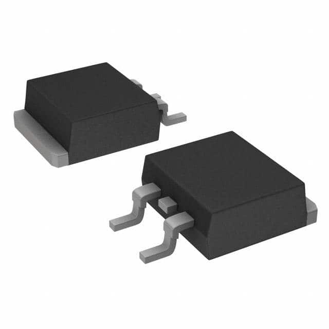
- Package: TO-263-3 (D2PAK)
- Essence: Efficient power management and control
- Packaging/Quantity: Typically packaged in reels or tubes, quantity varies by manufacturer
Specifications
- Voltage Rating: 100V
- Current Rating: 79A
- On-Resistance: 7.9 mΩ
- Gate Charge: 45nC
- Operating Temperature: -55°C to 175°C
- Mounting Type: Surface Mount
- Package / Case: TO-263-3
Detailed Pin Configuration
The IPB79CN10N G typically has three pins: 1. Gate (G): Input for controlling the switching operation 2. Drain (D): Output terminal connected to the load 3. Source (S): Ground reference for the MOSFET
Functional Features
- High voltage capability allows for use in various power applications
- Low on-resistance minimizes power losses and improves efficiency
- Fast switching speed enables rapid power control
Advantages and Disadvantages
Advantages
- Efficient power management
- Low power dissipation
- Fast response time
Disadvantages
- Sensitivity to static electricity
- Gate drive requirements
Working Principles
The IPB79CN10N G operates based on the principle of field-effect transistors, where the voltage applied to the gate terminal controls the flow of current between the drain and source terminals. By modulating the gate voltage, the MOSFET can effectively switch high-power loads on and off.
Detailed Application Field Plans
The IPB79CN10N G finds extensive use in the following applications: - Switching power supplies - Motor control - LED lighting - Audio amplifiers - Automotive systems
Detailed and Complete Alternative Models
Some alternative models to the IPB79CN10N G include: - IRFB7434PbF - FDP7030BL - IPP60R190E6
In conclusion, the IPB79CN10N G is a versatile power MOSFET with high voltage capability, low on-resistance, and fast switching speed, making it suitable for a wide range of electronic applications.
(Word count: 409)
Wymień 10 typowych pytań i odpowiedzi związanych z zastosowaniem IPB79CN10N G w rozwiązaniach technicznych
What is IPB79CN10N G?
- IPB79CN10N G is a high-power, N-channel MOSFET designed for various technical applications requiring efficient power management.
What are the key specifications of IPB79CN10N G?
- The key specifications include a maximum drain-source voltage of 100V, continuous drain current of 79A, low on-resistance, and fast switching capabilities.
In what technical solutions can IPB79CN10N G be used?
- IPB79CN10N G can be used in applications such as motor control, power supplies, DC-DC converters, and automotive systems.
How does IPB79CN10N G contribute to power management?
- IPB79CN10N G offers low on-resistance and high current-carrying capability, making it suitable for efficient power switching and management.
What are the thermal considerations for using IPB79CN10N G in technical solutions?
- Proper heat sinking and thermal management are important when using IPB79CN10N G to ensure optimal performance and reliability.
Does IPB79CN10N G require any specific gate drive requirements?
- IPB79CN10N G may have specific gate drive requirements, including voltage and current levels, to ensure proper switching and performance.
Are there any application notes or reference designs available for using IPB79CN10N G?
- Yes, application notes and reference designs are available to assist in the proper implementation of IPB79CN10N G in various technical solutions.
What protection features does IPB79CN10N G offer?
- IPB79CN10N G may offer protection features such as overcurrent protection, overtemperature protection, and ESD protection to enhance system reliability.
Can IPB79CN10N G be used in high-frequency switching applications?
- IPB79CN10N G's fast switching capabilities make it suitable for high-frequency switching applications, but proper design considerations are necessary.
Where can I find detailed technical documentation for IPB79CN10N G?
- Detailed technical documentation for IPB79CN10N G can be found on the manufacturer's website or through authorized distributors.