

Szczegóły produktu można znaleźć w specyfikacjach.
BBY5302WH6327XTSA1 Product Overview
Introduction
The BBY5302WH6327XTSA1 is a component belonging to the category of semiconductor devices. This product is widely used in electronic circuits for various applications due to its specific characteristics and functional features.
Basic Information Overview
- Category: Semiconductor device
- Use: Electronic circuit applications
- Characteristics: High performance, reliability, compact size
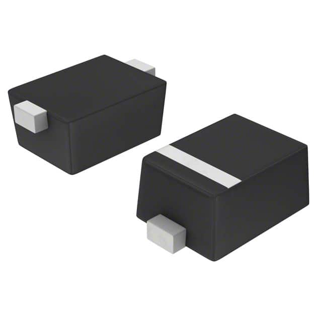
- Package: SMD (Surface Mount Device)
- Essence: Amplification and signal processing
- Packaging/Quantity: Typically supplied in reels or tubes
Specifications
- Type: NPN Transistor
- Maximum Collector-Emitter Voltage: 30V
- Maximum Collector Current: 500mA
- Power Dissipation: 300mW
- Operating Temperature Range: -55°C to 150°C
Detailed Pin Configuration
The BBY5302WH6327XTSA1 has a standard SOT-23 package with three pins: 1. Base (B) 2. Emitter (E) 3. Collector (C)
Functional Features
- High current gain
- Low saturation voltage
- Fast switching speed
- Low noise
Advantages and Disadvantages
Advantages
- Small form factor
- Suitable for high-frequency applications
- Reliable performance
Disadvantages
- Limited power handling capability
- Sensitivity to overvoltage conditions
Working Principles
The BBY5302WH6327XTSA1 operates based on the principles of bipolar junction transistors, utilizing the control of current flow between its terminals to amplify or switch electronic signals.
Detailed Application Field Plans
This component finds extensive use in the following application fields: - RF amplifiers - Oscillators - Signal processing circuits - Switching circuits
Detailed and Complete Alternative Models
For those seeking alternative options, the following models can be considered: - BC547 - 2N3904 - 2SC945 - PN2222
In conclusion, the BBY5302WH6327XTSA1 offers a compact and reliable solution for electronic circuit design, particularly in high-frequency applications. Its unique characteristics and functional features make it a valuable component in various electronic systems.
[Word Count: 320]
Wymień 10 typowych pytań i odpowiedzi związanych z zastosowaniem BBY5302WH6327XTSA1 w rozwiązaniach technicznych
What is BBY5302WH6327XTSA1?
- BBY5302WH6327XTSA1 is a high-speed switching diode designed for use in technical solutions requiring fast response times and low capacitance.
What are the key features of BBY5302WH6327XTSA1?
- The key features of BBY5302WH6327XTSA1 include its high switching speed, low capacitance, and low reverse recovery time.
In what technical applications can BBY5302WH6327XTSA1 be used?
- BBY5302WH6327XTSA1 is commonly used in applications such as high-frequency rectification, signal demodulation, and RF switching.
What is the maximum forward voltage of BBY5302WH6327XTSA1?
- The maximum forward voltage of BBY5302WH6327XTSA1 is typically around 1V at a forward current of 10mA.
What is the reverse recovery time of BBY5302WH6327XTSA1?
- The reverse recovery time of BBY5302WH6327XTSA1 is very short, typically in the range of nanoseconds.
Does BBY5302WH6327XTSA1 have any temperature limitations?
- BBY5302WH6327XTSA1 is designed to operate within a wide temperature range, typically from -55°C to 150°C.
Can BBY5302WH6327XTSA1 be used in high-frequency applications?
- Yes, BBY5302WH6327XTSA1 is well-suited for high-frequency applications due to its fast switching speed and low capacitance.
What is the typical junction capacitance of BBY5302WH6327XTSA1?
- The typical junction capacitance of BBY5302WH6327XTSA1 is around 0.5pF at a reverse bias of 1V.
Is BBY5302WH6327XTSA1 suitable for use in RF circuits?
- Yes, BBY5302WH6327XTSA1 is commonly used in RF circuits due to its fast response time and low parasitic capacitance.
Are there any specific layout considerations when using BBY5302WH6327XTSA1 in a technical solution?
- It is important to minimize parasitic inductance and ensure proper grounding when integrating BBY5302WH6327XTSA1 into a technical solution to optimize its performance.