

Szczegóły produktu można znaleźć w specyfikacjach.
ICS932S200BFLF
Overview
Category
ICS932S200BFLF belongs to the category of integrated circuits.
Use
ICS932S200BFLF is commonly used in electronic devices for signal processing and frequency synthesis.
Characteristics
- Signal processing and frequency synthesis capabilities
- Compact size and low power consumption
- High-speed data transmission
- Wide operating voltage range
Package
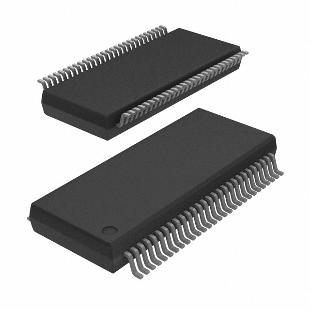
ICS932S200BFLF is available in a small form factor package, suitable for surface mount technology (SMT) assembly.
Essence
ICS932S200BFLF is an essential component in electronic systems that require precise signal processing and frequency synthesis.
Packaging/Quantity
ICS932S200BFLF is typically packaged in reels or trays, with quantities varying depending on customer requirements.
Specifications and Parameters
- Operating Voltage: 3.3V
- Frequency Range: 1Hz - 200MHz
- Input Clock Formats: LVCMOS, LVDS, HCSL
- Output Clock Formats: LVCMOS, LVDS, HCSL
- Temperature Range: -40°C to +85°C
- Package Type: QFN
Pin Configuration
The pin configuration of ICS932S200BFLF is as follows:
Pin 1: VDD
Pin 2: GND
Pin 3: CLK_IN
Pin 4: CLK_OUT
Pin 5: OE
Pin 6: NC
Pin 7: NC
Pin 8: NC
Functional Characteristics
ICS932S200BFLF offers the following functional characteristics:
- Clock input buffering and distribution
- Frequency multiplication and division
- Phase-locked loop (PLL) operation
- Output enable/disable control
Advantages and Disadvantages
Advantages
- High-performance signal processing
- Flexible clock input and output formats
- Wide operating temperature range
- Small form factor package
Disadvantages
- Limited frequency range (1Hz - 200MHz)
- Requires external power supply
Applicable Range of Products
ICS932S200BFLF is suitable for a wide range of electronic products, including:
- Communication equipment
- Computer peripherals
- Consumer electronics
- Industrial automation systems
- Medical devices
Working Principles
ICS932S200BFLF operates based on the principles of clock buffering, frequency synthesis, and phase-locked loop (PLL) control. It takes an input clock signal, processes it using internal circuitry, and generates an output clock signal with the desired frequency and format.
Detailed Application Field Plans
ICS932S200BFLF can be used in various applications, such as:
- Network routers: Provides precise clock synchronization for data transmission.
- Digital oscilloscopes: Enables accurate timebase generation for waveform analysis.
- Satellite communication systems: Facilitates reliable signal processing and frequency synthesis.
- Automotive electronics: Supports timing requirements for engine control units and infotainment systems.
- Test and measurement instruments: Ensures precise timing for accurate measurements.
Detailed Alternative Models
Some alternative models to ICS932S200BFLF include:
- ICS932S201BFLF
- ICS932S202BFLF
- ICS932S203BFLF
- ICS932S204BFLF
- ICS932S205BFLF
5 Common Technical Questions and Answers
Q: What is the maximum operating frequency of ICS932S200BFLF? A: The maximum operating frequency is 200MHz.
Q: Can I use LVDS input and LVCMOS output with ICS932S200BFLF? A: Yes, ICS932S200BFLF supports both LVDS and LVCMOS input/output formats.
Q: What is the power supply voltage for ICS932S200BFLF? A: The power supply voltage is 3.3V.
Q: Can I use ICS932S200BFLF in automotive applications? A: Yes, ICS932S200BFLF is suitable for automotive electronics.
Q: Does ICS932S200BFLF require an external crystal oscillator? A: No, ICS932S200BFLF has an internal phase-locked loop (PLL) for frequency synthesis.
This concludes the encyclopedia entry for ICS932S200BFLF.