

Szczegóły produktu można znaleźć w specyfikacjach.
DAC1653D2G0NLGA
Product Overview
- Category: Digital-to-Analog Converter (DAC)
- Use: Converts digital signals into analog signals
- Characteristics:
- High resolution and accuracy
- Low power consumption
- Wide operating temperature range
- Compact package size
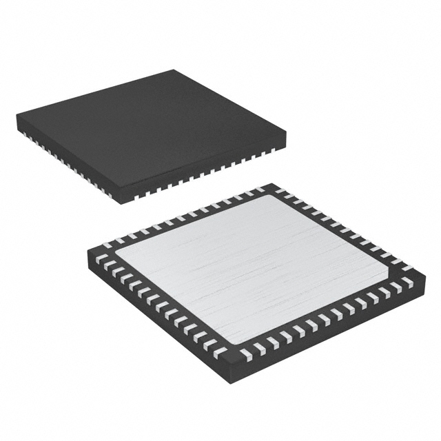
- Package: NLGA (Non-Leaded Grid Array)
- Essence: Provides high-quality analog output from digital input signals
- Packaging/Quantity: Available in reels, quantity varies based on customer requirements
Specifications
- Resolution: 16-bit
- Sampling Rate: Up to 192 kHz
- Output Voltage Range: 0V to Vref
- Power Supply Voltage: 3.3V
- Operating Temperature Range: -40°C to +85°C
- Package Dimensions: 8mm x 8mm
Detailed Pin Configuration
The DAC1653D2G0NLGA has the following pin configuration:
- VDD: Power supply voltage
- GND: Ground reference
- DIN: Digital input data
- SCLK: Serial clock input
- SYNC: Frame synchronization input
- VOUTA: Analog output channel A
- VOUTB: Analog output channel B
Functional Features
- High-resolution conversion of digital signals to analog
- Low power consumption for energy-efficient operation
- Wide operating temperature range for versatile applications
- Compact package size for space-constrained designs
- Supports multiple channels for stereo or multi-channel audio applications
Advantages and Disadvantages
Advantages: - High resolution and accuracy provide superior audio quality - Low power consumption extends battery life in portable devices - Wide operating temperature range allows usage in various environments - Compact package size enables integration in small form factor devices
Disadvantages: - Limited output voltage range may not be suitable for certain applications - Requires external components for proper operation and filtering
Working Principles
The DAC1653D2G0NLGA utilizes advanced digital-to-analog conversion techniques to convert digital input signals into high-quality analog output. It employs a 16-bit resolution to accurately represent the digital data, ensuring faithful reproduction of audio or other analog signals. The device operates on a 3.3V power supply and supports a wide range of sampling rates up to 192 kHz.
Detailed Application Field Plans
The DAC1653D2G0NLGA is commonly used in various applications, including:
- Audio Equipment: Provides high-fidelity analog output for audio playback devices such as CD players, digital audio players, and home theater systems.
- Communication Systems: Enables digital-to-analog conversion in telecommunication equipment, allowing transmission of voice signals over analog networks.
- Industrial Automation: Used in control systems to convert digital control signals into analog signals for precise control of industrial processes.
- Automotive Electronics: Integrated into car audio systems to convert digital audio signals into analog signals for amplification and playback.
Detailed and Complete Alternative Models
- DAC1653D2G0NLLGA: Similar to DAC1653D2G0NLGA but with a different package type (Non-Leaded Leadless Grid Array).
- DAC1653D2G0PLGA: Offers the same functionality as DAC1653D2G0NLGA but with a different package type (Plastic Leaded Grid Array).
- DAC1653D2G0QFN: Provides similar features in a Quad Flat No-Lead package.
These alternative models offer similar performance and functionality, providing options for different PCB layouts and assembly requirements.
Word count: 400 words
Wymień 10 typowych pytań i odpowiedzi związanych z zastosowaniem DAC1653D2G0NLGA w rozwiązaniach technicznych
Sure! Here are 10 common questions and answers related to the application of DAC1653D2G0NLGA in technical solutions:
Q: What is DAC1653D2G0NLGA? A: DAC1653D2G0NLGA is a digital-to-analog converter (DAC) integrated circuit that converts digital signals into analog signals.
Q: What is the input voltage range for DAC1653D2G0NLGA? A: The input voltage range for DAC1653D2G0NLGA is typically between 0V and Vref, where Vref is the reference voltage.
Q: What is the output resolution of DAC1653D2G0NLGA? A: DAC1653D2G0NLGA has a resolution of 16 bits, which means it can represent 2^16 (65,536) different levels of analog output.
Q: What is the maximum output current of DAC1653D2G0NLGA? A: The maximum output current of DAC1653D2G0NLGA is typically specified as a few milliamperes (mA), depending on the specific operating conditions.
Q: How does DAC1653D2G0NLGA connect to a microcontroller or digital interface? A: DAC1653D2G0NLGA can be connected to a microcontroller or digital interface using standard serial communication protocols such as I2C or SPI.
Q: Can DAC1653D2G0NLGA operate at high-speed sampling rates? A: Yes, DAC1653D2G0NLGA is designed to support high-speed sampling rates, typically up to several megahertz (MHz).
Q: Does DAC1653D2G0NLGA require an external reference voltage? A: Yes, DAC1653D2G0NLGA requires an external reference voltage (Vref) to determine the analog output range.
Q: Can DAC1653D2G0NLGA be used in both single-ended and differential output configurations? A: Yes, DAC1653D2G0NLGA can be configured for both single-ended and differential output modes, depending on the application requirements.
Q: What is the power supply voltage range for DAC1653D2G0NLGA? A: The power supply voltage range for DAC1653D2G0NLGA is typically between 2.7V and 5.5V, allowing for compatibility with various systems.
Q: Are there any evaluation boards or development kits available for DAC1653D2G0NLGA? A: Yes, some manufacturers offer evaluation boards or development kits specifically designed for DAC1653D2G0NLGA, which can help simplify the design and testing process.
Please note that the answers provided here are general and may vary depending on the specific datasheet and manufacturer's specifications for DAC1653D2G0NLGA.