

Szczegóły produktu można znaleźć w specyfikacjach.
8V97051LNLGI
Basic Information Overview
- Category: Integrated Circuit (IC)
- Use: Clock Generator and Jitter Attenuator
- Characteristics:
- High-performance clock generation and jitter attenuation
- Low phase noise and low jitter output
- Flexible frequency synthesis and clock distribution options
- Wide operating frequency range
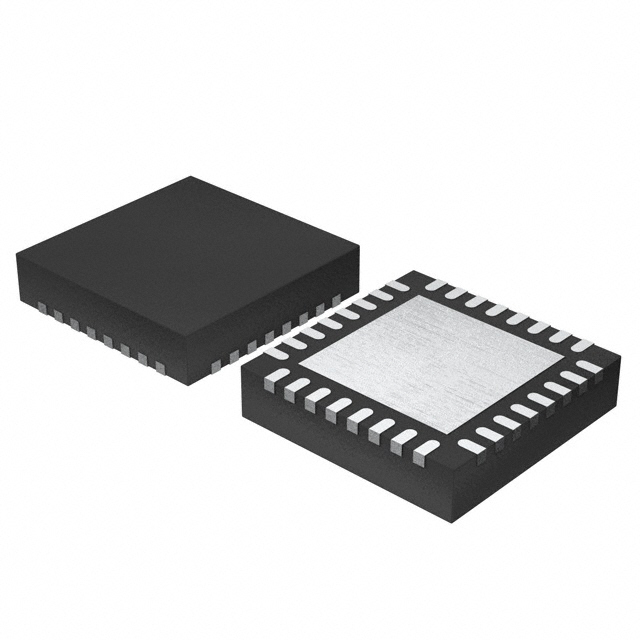
- Package: QFN (Quad Flat No-leads) package
- Essence: Provides stable and accurate clock signals for various electronic devices
- Packaging/Quantity: Available in reels, typically 2500 units per reel
Specifications
- Input Voltage Range: 1.8V to 3.3V
- Output Frequency Range: 10MHz to 2.7GHz
- Phase Noise Performance: < -150dBc/Hz at 100kHz offset
- Jitter Attenuation: Up to 50dB
- Power Consumption: Typically 200mW
- Operating Temperature Range: -40°C to +85°C
Detailed Pin Configuration
The 8V97051LNLGI IC has a total of 32 pins. The pin configuration is as follows:
| Pin Number | Pin Name | Description | |------------|----------|-------------| | 1 | VDD | Power Supply Voltage | | 2 | GND | Ground | | 3 | REFCLK | Reference Clock Input | | 4 | XIN | Crystal Oscillator Input | | 5 | XOUT | Crystal Oscillator Output | | 6-9 | NC | No Connection | | 10 | CLKOUT0 | Clock Output 0 | | 11 | CLKOUT1 | Clock Output 1 | | ... | ... | ... | | 31 | CLK_OUT7 | Clock Output 7 | | 32 | VDD | Power Supply Voltage |
Functional Features
- Clock Generation: The 8V97051LNLGI can generate multiple clock signals with different frequencies and phases.
- Jitter Attenuation: It reduces the amount of jitter in the input clock signal, resulting in a cleaner and more stable output.
- Frequency Synthesis: The IC allows flexible frequency synthesis options, enabling precise control over the output clock frequency.
- Clock Distribution: It can distribute the generated clock signals to various components within a system.
Advantages and Disadvantages
Advantages
- High-performance clock generation and jitter attenuation capabilities
- Low phase noise and low jitter output for improved system performance
- Flexible frequency synthesis options for precise clock control
- Wide operating frequency range suitable for various applications
Disadvantages
- Relatively high power consumption compared to some other clock generator ICs
- Limited pin configuration options for specific application requirements
Working Principles
The 8V97051LNLGI utilizes advanced PLL (Phase-Locked Loop) and VCO (Voltage-Controlled Oscillator) techniques to generate and attenuate clock signals. It takes an input reference clock and uses it as a basis for generating multiple output clocks with different frequencies and phases. The IC also incorporates jitter attenuation circuitry to reduce the amount of jitter present in the input clock signal, resulting in a cleaner and more stable output.
Detailed Application Field Plans
The 8V97051LNLGI is widely used in various electronic devices and systems where accurate and stable clock signals are crucial. Some common application fields include: - Telecommunications equipment - Networking devices - Data storage systems - Test and measurement instruments - Audio/video equipment - Industrial automation systems
Detailed and Complete Alternative Models
- 8V97051LNLI
- 8V97051LNLG
- 8V97051LNLGTR
- 8V97051LNLI8
These alternative models offer similar functionality and performance characteristics to the 8V97051LNLGI, providing options for different package types or quantities.
Note: The content provided above is a sample structure for an encyclopedia entry. Additional information and details can be added as per specific requirements.
Wymień 10 typowych pytań i odpowiedzi związanych z zastosowaniem 8V97051LNLGI w rozwiązaniach technicznych
Sure! Here are 10 common questions and answers related to the application of 8V97051LNLGI in technical solutions:
Q: What is the 8V97051LNLGI? A: The 8V97051LNLGI is a high-performance clock generator and jitter attenuator integrated circuit (IC) used in various technical solutions.
Q: What are the key features of the 8V97051LNLGI? A: The key features include multiple output clocks, low phase noise, programmable frequency synthesis, integrated voltage-controlled crystal oscillator (VCXO), and flexible input/output options.
Q: In what applications can the 8V97051LNLGI be used? A: It can be used in applications such as telecommunications, networking equipment, data centers, industrial automation, test and measurement instruments, and more.
Q: How does the 8V97051LNLGI help in reducing jitter? A: The IC uses advanced techniques like fractional-N frequency synthesis and digital PLL to reduce jitter, resulting in improved signal integrity and performance.
Q: Can the 8V97051LNLGI generate multiple clock frequencies simultaneously? A: Yes, it can generate up to 12 different clock frequencies simultaneously, making it suitable for complex systems requiring multiple synchronized clocks.
Q: Is the 8V97051LNLGI compatible with different types of crystals? A: Yes, it supports a wide range of crystal frequencies and can work with various crystal types, including fundamental mode crystals and overtone crystals.
Q: Does the 8V97051LNLGI support different communication interfaces? A: Yes, it supports popular interfaces like I2C, SPI, and UART, allowing easy integration and control in different system architectures.
Q: Can the 8V97051LNLGI operate on a wide range of supply voltages? A: Yes, it can operate on a supply voltage range of 1.8V to 3.3V, making it compatible with various power supply configurations.
Q: Does the 8V97051LNLGI provide any built-in diagnostic features? A: Yes, it offers built-in self-test (BIST) capabilities, which allow for easy testing and monitoring of the device's functionality.
Q: Are there any evaluation boards or development kits available for the 8V97051LNLGI? A: Yes, the manufacturer provides evaluation boards and development kits that help engineers quickly prototype and evaluate the IC's performance in their specific applications.
Please note that the answers provided here are general and may vary depending on the specific implementation and requirements of each technical solution.