

Szczegóły produktu można znaleźć w specyfikacjach.
8T49N241-994NLGI
Basic Information Overview
- Category: Integrated Circuit (IC)
- Use: Clock Generator and Jitter Attenuator
- Characteristics: High-performance, low-jitter clock generation and distribution solution
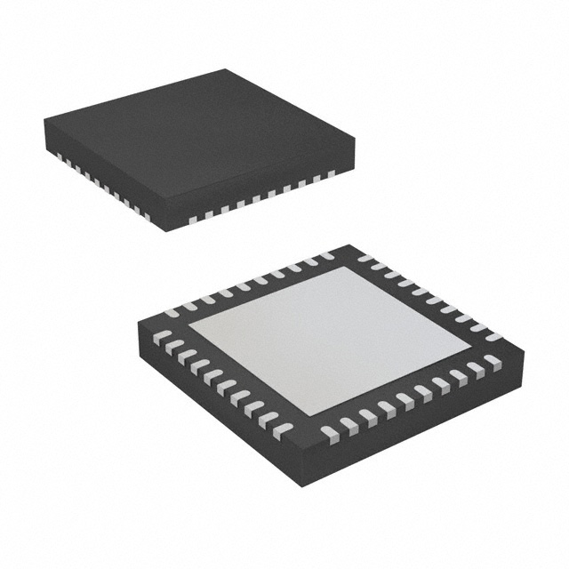
- Package: 48-pin QFN package
- Essence: Provides precise clock signals for various applications
- Packaging/Quantity: Available in reels of 250 units
Specifications
- Input Voltage Range: 1.8V to 3.3V
- Output Frequency Range: 0.01Hz to 350MHz
- Number of Outputs: 4 differential or 8 single-ended
- Output Types: LVPECL, LVDS, HCSL, CMOS
- Phase Noise Performance: Excellent phase noise characteristics
- Operating Temperature Range: -40°C to +85°C
Detailed Pin Configuration
The 8T49N241-994NLGI IC has a total of 48 pins. The pin configuration is as follows:
- VDDO1
- VSSO1
- OUT0_N
- OUT0_P
- VDDO2
- VSSO2
- OUT1_N
- OUT1_P
- VDDO3
- VSSO3
- OUT2_N
- OUT2_P
- VDDO4
- VSSO4
- OUT3_N
- OUT3_P
- VDDI
- VSSI
- SDA
- SCL
- VDDA
- VSSA
- XTALI
- XTALO
- VDDREF
- VSSREF
- REFOUT_N
- REFOUT_P
- VDDPLL
- VSSPLL
- PLL_SDA
- PLL_SCL
- VDDOSC
- VSSOSC
- OSC_SDA
- OSC_SCL
- VDDREG
- VSSREG
- REG_SDA
- REG_SCL
- VDDIO
- VSSIO
- IO0
- IO1
- IO2
- IO3
- VDD
- VSS
Functional Features
- Clock Generation: The 8T49N241-994NLGI IC generates high-quality clock signals with low jitter for precise timing requirements.
- Jitter Attenuation: It also includes a jitter attenuator function, which reduces the phase noise and jitter of incoming clock signals.
- Multiple Output Formats: The IC supports various output types, including LVPECL, LVDS, HCSL, and CMOS, providing flexibility for different applications.
- Frequency Flexibility: With a wide output frequency range from 0.01Hz to 350MHz, it can cater to diverse frequency requirements.
Advantages and Disadvantages
Advantages: - High-performance clock generation and distribution solution - Excellent phase noise characteristics - Wide operating temperature range - Multiple output formats for versatility
Disadvantages: - Limited number of outputs (4 differential or 8 single-ended) - Requires careful consideration of power supply voltage compatibility
Working Principles
The 8T49N241-994NLGI IC utilizes advanced clock synthesis and jitter attenuation techniques. It incorporates a phase-locked loop (PLL) to generate precise clock signals based on an external reference input. The PLL ensures that the output clock signals have minimal phase noise and jitter.
The IC also features a flexible input interface that accepts various input formats and frequencies. It employs sophisticated algorithms to attenuate the jitter and phase noise of incoming clock signals, resulting in cleaner and more stable output clocks.
Detailed Application Field Plans
The 8T49N241-994NLGI IC finds applications in various fields where accurate and reliable clock signals are crucial. Some potential application areas include: 1. Telecommunications: Clock synchronization in network equipment, routers, and switches. 2. Data Centers: Timing solutions for servers, storage systems, and high-speed interconnects. 3. Industrial Automation: Precise timing for control systems, PLCs, and robotics. 4. Test and Measurement: Clock generation for oscilloscopes, signal generators, and data acquisition systems. 5. Broadcast and Audio/Video: Synchronization of video processing equipment, audio codecs, and broadcast infrastructure.
Detailed and Complete Alternative Models
- 8T49N240-994NLGI: Similar to 8T49N241-994NLGI but with 2 differential or 4 single-ended outputs.
- 8T49N242-994NLGI: Enhanced version with additional features such as frequency margining and spread spectrum support.
- 8
Wymień 10 typowych pytań i odpowiedzi związanych z zastosowaniem 8T49N241-994NLGI w rozwiązaniach technicznych
Sure! Here are 10 common questions and answers related to the application of 8T49N241-994NLGI in technical solutions:
Q: What is the purpose of the 8T49N241-994NLGI in technical solutions? A: The 8T49N241-994NLGI is a component used for clock generation and synchronization in various technical applications.
Q: What is the operating voltage range of the 8T49N241-994NLGI? A: The 8T49N241-994NLGI operates within a voltage range of 1.71V to 3.63V.
Q: Can the 8T49N241-994NLGI be used in battery-powered devices? A: Yes, the 8T49N241-994NLGI can be used in battery-powered devices as it operates within a low voltage range.
Q: What is the frequency range supported by the 8T49N241-994NLGI? A: The 8T49N241-994NLGI supports a wide frequency range from 0.1Hz to 350MHz.
Q: Does the 8T49N241-994NLGI support multiple clock outputs? A: Yes, the 8T49N241-994NLGI supports up to 12 clock outputs, making it suitable for complex systems.
Q: Can the 8T49N241-994NLGI generate spread spectrum clocking (SSC) signals? A: Yes, the 8T49N241-994NLGI has built-in spread spectrum modulation capability for reducing electromagnetic interference (EMI).
Q: Is the 8T49N241-994NLGI programmable? A: Yes, the 8T49N241-994NLGI is programmable through an I2C interface, allowing for flexible configuration.
Q: What are the typical applications of the 8T49N241-994NLGI? A: The 8T49N241-994NLGI is commonly used in networking equipment, telecommunications systems, industrial automation, and high-speed data interfaces.
Q: Does the 8T49N241-994NLGI have any integrated fail-safe features? A: Yes, the 8T49N241-994NLGI includes a fail-safe mechanism that ensures a stable output clock signal even in case of input signal loss.
Q: Can the 8T49N241-994NLGI be used in automotive applications? A: Yes, the 8T49N241-994NLGI is qualified for automotive applications and meets the necessary standards for reliability and performance.
Please note that these answers are general and may vary depending on the specific requirements and use cases. It's always recommended to refer to the datasheet or consult with the manufacturer for detailed information.