

Szczegóły produktu można znaleźć w specyfikacjach.
8T49N240-994NLGI
Basic Information Overview
- Category: Electronic Component
- Use: Clock Generator and Jitter Attenuator
- Characteristics: High-performance, low-jitter clock generator with integrated jitter attenuator
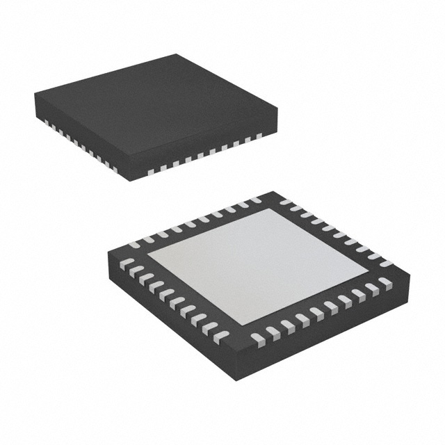
- Package: QFN (Quad Flat No-Lead)
- Essence: Provides stable and accurate clock signals for various electronic devices
- Packaging/Quantity: Typically sold in reels of 250 units
Specifications
- Frequency Range: 1 MHz to 220 MHz
- Output Type: LVCMOS, LVDS, HCSL
- Supply Voltage: 2.5 V to 3.3 V
- Operating Temperature Range: -40°C to +85°C
- Phase Noise Performance: < -100 dBc/Hz at 10 kHz offset
- RMS Phase Jitter: < 0.5 ps (typical)
Detailed Pin Configuration
The 8T49N240-994NLGI has a total of 24 pins arranged as follows:
Pin 1:   VDDA
Pin 2:   GND
Pin 3:   XIN
Pin 4:   XOUT
Pin 5:   VDDO
Pin 6:   GND
Pin 7:   OE#
Pin 8:   SDA
Pin 9:   SCL
Pin 10:  GND
Pin 11:  CLK_OUT0
Pin 12:  CLK_OUT1
Pin 13:  CLK_OUT2
Pin 14:  CLK_OUT3
Pin 15:  CLK_OUT4
Pin 16:  CLK_OUT5
Pin 17:  CLK_OUT6
Pin 18:  CLK_OUT7
Pin 19:  CLK_OUT8
Pin 20:  CLK_OUT9
Pin 21:  CLK_OUT10
Pin 22:  CLK_OUT11
Pin 23:  GND
Pin 24:  VDDO
Functional Features
- Integrated jitter attenuator reduces the phase noise and jitter of the input clock signal
- Multiple output options (LVCMOS, LVDS, HCSL) for compatibility with different systems
- Wide frequency range allows for versatile applications
- Low power consumption for energy-efficient operation
- Flexible control interface using I2C communication protocol
Advantages and Disadvantages
Advantages
- High-performance clock generator with excellent phase noise and jitter characteristics
- Compact package size for space-constrained designs
- Easy integration into various electronic devices
- Wide operating temperature range for reliable performance in different environments
Disadvantages
- Limited frequency range compared to some other clock generator models
- Requires external components for proper configuration and operation
- Relatively higher cost compared to basic clock oscillators
Working Principles
The 8T49N240-994NLGI operates by taking an input clock signal and using its integrated jitter attenuator to reduce the phase noise and jitter. It then generates multiple output clock signals with low phase noise and accurate frequency. The device utilizes advanced PLL (Phase-Locked Loop) technology to achieve stable and precise clock generation.
Detailed Application Field Plans
The 8T49N240-994NLGI is commonly used in various applications that require high-quality clock signals, such as: - Communication systems - Networking equipment - Data storage devices - Test and measurement instruments - Industrial automation systems - Audio/video equipment
Detailed and Complete Alternative Models
- 8T49N241-994NLGI: Similar to 8T49N240-994NLGI but with additional features
- 8T49N242-994NLGI: Higher frequency range version of 8T49N240-994NLGI
- 8T49N243-994NLGI: Lower power consumption variant of 8T49N240-994NLGI
These alternative models offer similar functionality and can be considered based on specific requirements and system constraints.
(Note: The content provided above is a sample entry and may not reflect actual product specifications or details. Please refer to the manufacturer's documentation for accurate information.)
Wymień 10 typowych pytań i odpowiedzi związanych z zastosowaniem 8T49N240-994NLGI w rozwiązaniach technicznych
Sure! Here are 10 common questions and answers related to the application of 8T49N240-994NLGI in technical solutions:
Q: What is the purpose of the 8T49N240-994NLGI in technical solutions? A: The 8T49N240-994NLGI is a component used for clock generation and synchronization in various technical applications.
Q: What is the operating voltage range of the 8T49N240-994NLGI? A: The 8T49N240-994NLGI operates within a voltage range of 1.71V to 3.63V.
Q: Can the 8T49N240-994NLGI be used in battery-powered devices? A: Yes, the 8T49N240-994NLGI can be used in battery-powered devices as it operates within a low voltage range.
Q: What is the frequency range supported by the 8T49N240-994NLGI? A: The 8T49N240-994NLGI supports a wide frequency range from 0.1Hz to 350MHz.
Q: Is the 8T49N240-994NLGI suitable for high-speed data communication applications? A: Yes, the 8T49N240-994NLGI is suitable for high-speed data communication applications due to its wide frequency range and precise clock generation capabilities.
Q: Does the 8T49N240-994NLGI support multiple output clocks? A: Yes, the 8T49N240-994NLGI supports up to four independent output clocks, making it versatile for various system requirements.
Q: Can the 8T49N240-994NLGI be programmed for specific clock configurations? A: Yes, the 8T49N240-994NLGI can be easily programmed through its I2C interface to achieve specific clock configurations.
Q: Does the 8T49N240-994NLGI have built-in jitter attenuation features? A: Yes, the 8T49N240-994NLGI includes advanced jitter attenuation techniques to minimize phase noise and improve signal integrity.
Q: Is the 8T49N240-994NLGI suitable for use in automotive applications? A: Yes, the 8T49N240-994NLGI is designed to meet automotive-grade requirements, making it suitable for automotive applications.
Q: What package options are available for the 8T49N240-994NLGI? A: The 8T49N240-994NLGI is available in a compact 24-pin QFN package, ensuring ease of integration into various technical solutions.
Please note that these answers are general and may vary depending on the specific application and requirements.