

Szczegóły produktu można znaleźć w specyfikacjach.
AS7C325632-10BIN
Product Overview
Category
AS7C325632-10BIN belongs to the category of semiconductor memory products.
Use
It is primarily used as a random access memory (RAM) component in electronic devices.
Characteristics
- High-speed operation
- Low power consumption
- Large storage capacity
- Reliable performance
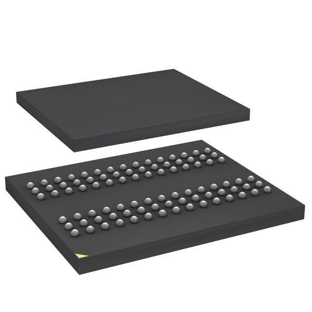
Package
AS7C325632-10BIN is available in a compact and durable package, suitable for surface mount technology (SMT) applications.
Essence
The essence of AS7C325632-10BIN lies in its ability to provide fast and efficient data storage and retrieval functions.
Packaging/Quantity
This product is typically packaged in reels or trays, with varying quantities depending on customer requirements.
Specifications
- Part Number: AS7C325632-10BIN
- Organization: 32M x 32
- Access Time: 10ns
- Voltage Supply: 3.3V
- Operating Temperature Range: -40°C to +85°C
- Package Type: BGA (Ball Grid Array)
- Pin Count: 119
Detailed Pin Configuration
The pin configuration of AS7C325632-10BIN is as follows:
- VDDQ
- DQ0
- DQ1
- DQ2
- DQ3
- DQ4
- DQ5
- DQ6
- DQ7
- DQ8
- DQ9
- DQ10
- DQ11
- DQ12
- DQ13
- DQ14
- DQ15
- DQ16
- DQ17
- DQ18
- DQ19
- DQ20
- DQ21
- DQ22
- DQ23
- DQ24
- DQ25
- DQ26
- DQ27
- DQ28
- DQ29
- DQ30
- DQ31
- A0
- A1
- A2
- A3
- A4
- A5
- A6
- A7
- A8
- A9
- A10
- A11
- A12
- A13
- A14
- A15
- A16
- A17
- A18
- A19
- A20
- A21
- A22
- A23
- A24
- A25
- A26
- A27
- A28
- A29
- A30
- A31
- /WE
- /CAS
- /RAS
- /CS0
- /CS1
- /CS2
- /CS3
- /OE
- /LB
- /UB
- /CE
- /ZZ
- VSS
- VDD
Functional Features
- High-speed data access and retrieval
- Low power consumption in standby mode
- Easy integration into various electronic systems
- Reliable operation under different environmental conditions
- Support for multiple chip select signals for flexible memory expansion
Advantages and Disadvantages
Advantages
- Fast access time enhances overall system performance
- Large storage capacity allows for extensive data storage
- Low power consumption prolongs battery life in portable devices
- Reliable operation ensures data integrity and system stability
Disadvantages
- Higher cost compared to other memory technologies
- Limited scalability beyond a certain storage capacity
- Sensitivity to electrostatic discharge (ESD) requires proper handling during installation and maintenance
Working Principles
AS7C325632-10BIN operates based on the principles of dynamic random access memory (DRAM). It stores data in capacitors within each memory cell, which need to be periodically refreshed to maintain data integrity. The memory controller sends commands and addresses to access specific data stored in the memory array.
Detailed Application Field Plans
AS7C325632-10BIN finds applications in various electronic devices, including but not limited to: - Personal computers - Servers - Networking equipment - Consumer electronics - Automotive systems - Industrial control systems
Detailed and Complete Alternative Models
Some alternative models that can be considered as alternatives to AS7C325632-10BIN are: - AS7C325632-12BIN - AS7C325632-15BIN - AS7C325632-
Wymień 10 typowych pytań i odpowiedzi związanych z zastosowaniem AS7C325632-10BIN w rozwiązaniach technicznych
Sure! Here are 10 common questions and answers related to the application of AS7C325632-10BIN in technical solutions:
Question: What is AS7C325632-10BIN?
Answer: AS7C325632-10BIN is a specific model of synchronous static random-access memory (SRAM) chip.Question: What is the capacity of AS7C325632-10BIN?
Answer: AS7C325632-10BIN has a capacity of 32 megabits (4 megabytes).Question: What is the operating voltage range for AS7C325632-10BIN?
Answer: AS7C325632-10BIN operates within a voltage range of 2.3V to 3.6V.Question: What is the access time of AS7C325632-10BIN?
Answer: AS7C325632-10BIN has an access time of 10 nanoseconds.Question: Can AS7C325632-10BIN be used in battery-powered devices?
Answer: Yes, AS7C325632-10BIN's low operating voltage range makes it suitable for battery-powered devices.Question: What is the pin configuration of AS7C325632-10BIN?
Answer: AS7C325632-10BIN has a 119-ball BGA (Ball Grid Array) package with specific pin assignments.Question: Is AS7C325632-10BIN compatible with standard microcontrollers?
Answer: Yes, AS7C325632-10BIN can be interfaced with standard microcontrollers using appropriate protocols.Question: Can AS7C325632-10BIN be used in high-speed data processing applications?
Answer: Yes, AS7C325632-10BIN's access time of 10 nanoseconds makes it suitable for high-speed data processing.Question: Does AS7C325632-10BIN support simultaneous read and write operations?
Answer: Yes, AS7C325632-10BIN supports simultaneous read and write operations.Question: Are there any specific temperature requirements for AS7C325632-10BIN?
Answer: AS7C325632-10BIN operates within a temperature range of -40°C to +85°C.
Please note that the answers provided here are general and may vary depending on the specific application and requirements.